Recent Content

Altera TSE driver and example program for lwIP (1.3.2)
After many many requests and complaints about lack of support and/or documentation for support of lwIP for the Altera TSE, I have developed a drop-in TSE driver and example program and made this available to the NIOS II community. This was done for NIOS II 8.1 SP0.01. I don't expect difficulty with version 9.x. This is for the latest version of lwIP (the latest is as of this post) for a minimal program and HTTP server based on the http server in the lwIP contrib folder. The lwIP TSE driver uses the altera_avalon_tse driver and SGDMA as-is. There is a complete (as in 41-step) set of instructions on creating the project and example program. More information and the link to the driver is available here: http://lwip.wikia.com/wiki/available_device_drivers#lwip_1.3.2 Please direct any questions, changes for NIOS II 9.1, or comments to this thread. 12-16-2010 update: This example works with NIOS Version 10.0 with some tweaks to the procedure to create the project. Also, a lwIP 1.4 release candidate has been out for a while and it drops into this example (in place of 1.3) without changes. Bill42KViews0likes257CommentsTutorial: Using the USB-Blaster as an SOPC/Qsys Avalon-MM master
Hi all, I've put together a tutorial on how to use the Altera JTAG-to-Avalon-MM master and Altera Verification IP Avalon-MM BFM Master under both SOPC builder and Qsys. http://www.ovro.caltech.edu/~dwh/correlator/pdf/altera_jtag_to_avalon_mm_tutorial.pdf (http://www.ovro.caltech.edu/%7edwh/correlator/pdf/altera_jtag_to_avalon_mm_tutorial.pdf) http://www.ovro.caltech.edu/~dwh/correlator/pdf/altera_jtag_to_avalon_mm_tutorial.zip (http://www.ovro.caltech.edu/%7edwh/correlator/pdf/altera_jtag_to_avalon_mm_tutorial.zip) The tutorial walks the user through the creation of an SOPC or Qsys system design, and provides scripts that automate the re-generation of the system. The tutorial shows how to simulate using Modelsim-ASE, and shows how to communicate with the hardware using System Console, quartus_stp, and then how to run a TCP/IP server under System Console or quartus_stp, and then communicate with that server from client code written in Tcl/Tk (a simple GUI) and a command-line C interface. Let me know if you like it, or have feedback/suggestions on how to improve the document. Cheers, Dave28KViews0likes119Comments
Is anybody else completely dissatisfied with this new forum?
This used to be a robust forum, lots of new questions everyday and, most impotantly, lots of responses. This new forum is clunky and time consuming to navigate. Nobody seems interested anymore. I used to check-in everyday to see what's new. Not any more.42KViews15likes119Comments- 19KViews0likes107Comments
Simple Socket Server on DE2 w/Davicom DM9000A
updated. Altera's Simple Socket Server demo running on a DE2 board with the Davicom DM9000a driver. here it is....zipped downloaded project source for sss on the de2 board. download link currently unavailable. Includes: - Hardware design (TLD in schematic block diagram format) - Programmable .SOF (time-limited, as developed in Quartus Web Edition v9.2) - SOPC builder system file - DM9000A driver for Nichestack TCP/IP stack / Altera HAL environment (courtesy of Columbia Uni) - Simple socket server software Simply... - (1) Download the .SOF in Quartus Programmer - (2) Open the software workspace in the "/software" directory in Nios II Build Tools (Eclipse IDE) - (3) Open Run >> Run Configurations. Delete the current configuration. Create a new launch configuration selecting the project name under the Project Tab. Ensure your DE2 board is plugged into USB. Check the target connection tab and make sure it is present. - (4) Plug into your local network (DHCP is enabled, or app will default to static IP) - (5) View the Nios II console for debugging information (via JTAG UART) - (6) Telnet into the board from a pc: telnet <ip address> 30. Enjoy the simple socket server demo from Altera! Questions/comments? Fire away below!12KViews0likes98CommentsLinux with MMU on NEEK
Hi, all. I'm testing Linux MMU version, on my NEEK. http://www.nioswiki.com/linux It works fine and I can use "bash" shell. This is the evident proof that we are using the true 'fork' instead of 'vfork'. May be this will depends on the version, but TSE driver claims an error and doesn't work on this design. The error is ERROR: altera_tse.c:1666: request_mem_region() failed I think that this error is caused by misunderstanding of the usage for the function request_mem_region(). Inside of the request_mem_region(), the function __request_region() is called. If the resource has been already registered, this function returns a non-NULL value, that is the pointer for its resource. But the resource 'sgdma_rx_base' is already registered in the initialization process, so this function returns the 'conflict' and if (!request_mem_region(sgdma_rx_base, sgdma_rx_size, "altera_tse")) { is always true. So I made a dirty patch, if (!request_mem_region(sgdma_rx_base, sgdma_rx_size, "altera_tse")) { reg_resource = __request_region(&iomem_resource, sgdma_rx_base, sgdma_rx_size, "altera_tse", 0); if (reg_resource != NULL && reg_resource->flags & IORESOURCE_BUSY) { printk(KERN_ERR "ERROR: %s:%d: request_mem_region() failed\n", __FILE__, __LINE__); ret = -EBUSY; goto out_sgdma_rx; } } Moreover, the author is forgetting that the DMA is working in the physical address world, so we need to set the pointers of descripters like // desc->source = read_addr; desc->source = virt_to_phys(read_addr); // desc->destination = write_addr; desc->destination = virt_to_phys(write_addr); // desc->next = (unsigned int *)next; desc->next = (unsigned int *)((unsigned long)next & 0x1fffffffUL); and so on. Also the frame buffer fb0 will not work well, because the driver 'altfb.c' is not implemented for Linux with MMU version. So I put some codes for altfb_mmap(), like /* We implement our own mmap to set MAY_SHARE and add the correct size */ static int altfb_mmap(struct fb_info *info, struct vm_area_struct *vma) { unsigned long phys_addr, phys_size; unsigned long addr; unsigned long size = vma->vm_end - vma->vm_start; unsigned long offset = vma->vm_pgoff << PAGE_SHIFT; // vma->vm_flags |= VM_MAYSHARE | VM_SHARED; // vma->vm_start = info->screen_base; // vma->vm_end = vma->vm_start + info->fix.smem_len; /* check range */ if (vma->vm_pgoff > (~0UL >> PAGE_SHIFT)) return -EINVAL; if (offset + size > altfb_fix.smem_len) return -EINVAL; vma->vm_flags |= VM_IO | VM_RESERVED; addr = vma->vm_start; phys_addr = altfb_fix.smem_start + offset; if ((offset + size) < altfb_fix.smem_len) phys_size = size; else phys_size = altfb_fix.smem_len - offset; vma->vm_page_prot = __pgprot(_PAGE_PRESENT|_PAGE_READ|_PAGE_WRITE); if (remap_pfn_range(vma, addr, phys_addr >> PAGE_SHIFT, phys_size, vma->vm_page_prot)) return -EAGAIN; return 0; } and rewrite the DMA descripters like desc->next = (void *)virt_to_phys((desc + 1)); So now, I can evoke telnetd and control NEEK through ethernet, and use Nano-X on Linux MMU version, but can't enter ftp session, because 'getservbyname()' function will not work well. I don't know the directory that the souce of 'getservbyname()' is included. Would anyone please tell me where is it? Thank you, in advance.5.9KViews0likes95CommentsDE2_UDP example for download here free (feedbacks are wellcomed)
Hi all. My goal is to get about 3Mbytes/sec data transfer rate from my DE2 board to PC. Here in this example I get about 1.2 Mbytes/sec. I'll accept comments about, how to speed up this, as well as suggests to improve the code, and some feedback from people that have interest in this theme. Could be in this thread or private. You can download the full project from: http://www.btxsistemas.com.ar/net2.zip I've used Quartus II 7.2 full suite. And the Wireshark software (http://www.wireshark.org/) like a net sniffer, but also, I've included in the main project folder, a UDP reciever to test the comunication between the DE2 board and the PC, if you wont to download the wireshark. Don't forget to specify your IP address and your MAC address in the NIOS hello_word "C" code to get it work properly. The main project is a modification of the DE2_NET demostration code that comes with the DE2 board. Have fun, and I'll be waiting for some comments.10KViews0likes94Commentscontinuous averaging using VHDL
I have a question related to VHDL programming. I want to calculate the continuous average. My example code is: process (clk, reset) begin if (reset = '1') then state<=idle; out-val=0; elsif(rising_edge(clk)) then case state is when idle => if req='1' then state= out-1; end if; when out-1 => if done='1' then out-val<=data-in (11 downto 0) state <= done-st; endif; when done-st => ack <='1'; state <= idle; when others => state <= idle; end case; end if; end process; On every positive edge of clock, the value of "out-val" changes. I want to continuously take the average of "out-val". I want to take average of 32 values continuously. Is there a way where I can take average of 32 values continuously till the clock is running. Kindly let me know how can I do that. You can modify the above code as well. Many Thanks,18KViews0likes90Comments
Featured Places
Community Resources
Check out the support articles on personalizing your community account, contributing to the community, and providing community feedback directly to the admin team!Tags
- troubleshooting10,401 Topics
- fpga dev tools quartus® prime software pro4,353 Topics
- FPGA Dev Tools Quartus II Software3,131 Topics
- stratix® 10 fpgas and socs1,552 Topics
- agilex® 7 fpgas and socs1,546 Topics
- arria® 10 fpgas and socs1,381 Topics
- stratix® v fpgas1,315 Topics
- arria® v fpgas and socs1,229 Topics
- Configuration1,095 Topics
- cyclone® v fpgas and socs1,058 Topics
Recent Blogs
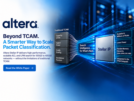
PACKET CLASSIFICATION | FPGA | NETWORKING + SECURITY Every packet decision starts with classification. Routers, firewalls, SmartNICs, security gateways, and service-edge platforms must determine which policy applies before traffic can be forwarded, blocked, inspected, redirected, or prioritized. TCAM earned its place in these systems because it provides predictable lookup behavior and native ternary matching for ACL and LPM workloads. But as policy databases grow, search keys widen, and rules change more frequently, the traditional approach of scaling specialized ternary memory creates tougher tradeoffs in capacity, power, resource utilization, and system integration. Altera Stellar solutions takes a different approach. Instead of scaling packet classification by building ever-larger ternary-memory structures, Stellar turns classification into an optimized search problem that runs on configurable FPGA resources. The result is an FPGA-native path for large, dynamic packet-classification tables without giving up the policy semantics that made TCAM useful in the first place. TCAM scales through memory expansion. Stellar scales through search intelligence. Keep the TCAM semantics. Change the scaling model. Stellar preserves the intent of ACL, LPM, and multi-field classification, but changes how those rules are represented and searched. The Stellar Software Stack organizes policies into optimized graph structures, partitions the rule database, and continuously manages those search structures as the database evolves. The hardware then executes the search using configurable FPGA search engines while rule information is stored in conventional memory resources. Depending on the configuration, Stellar can use on-chip M20K memory, eSRAM, DDR, or HBM. That gives architects more freedom to balance throughput, capacity, latency, power, and FPGA resource use around the needs of the actual system. Use dense memory where it makes sense, and intelligence where it matters A traditional TCAM combines storage and comparison circuitry inside specialized ternary-memory arrays. That architecture delivers deterministic matching, but scaling the table means scaling the specialized comparison structure as well. Stellar separates rule storage from search execution. Ternary information can be represented as value-and-mask data in conventional memory, while graph organization and software-managed optimization direct each search toward the relevant parts of the database. As tables grow from thousands of entries toward hundreds of thousands or millions, this creates a different path for scaling capacity and power. The white paper goes deeper into why this matters, including the tradeoffs between TCAM and Stellar, the role of memory hierarchy, and a set of Stellar configurations spanning different key widths, capacities, memory resources, and projected five-tuple performance. Bring classification into the programmable datapath The value is bigger than the lookup engine itself. Stellar is designed to operate inside the FPGA alongside packet parsing, telemetry, encryption, traffic management, host-interface logic, and customer packet-processing RTL. For system architects, that means classification can become part of the same programmable platform already handling the datapath. A firewall can pair large, dynamic ACL processing with the rest of its traffic pipeline. A router can combine LPM and policy enforcement with programmable networking functions. A SmartNIC can integrate flow classification with offload and customer-specific acceleration. That system-level flexibility is especially relevant for 100GE to 400GE designs where classification must scale without consuming the platform that surrounds it. Read the full whitepaper! The full Altera white paper, Altera TCAM Alternative Solutions Scale Packet Classification to Millions of Rules for Networking Equipment, explains the architecture behind Stellar and the design choices that make it different. It covers TCAM fundamentals and scaling limits, Stellar graph-based search and software partitioning, memory-hierarchy options, configuration examples, quantitative architectural comparisons, dynamic updates, and deployment use cases across networking and security. Read the white paper See how Stellar uses search intelligence, configurable FPGA resources, and a flexible memory hierarchy to create a scalable alternative for large ACL and LPM workloads.
17 days ago0likes
4 MIN READ
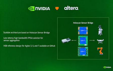
September 28, 2026 The next generation of embedded systems will not be defined by compute alone. It will depend on how quickly, reliably, and intelligently systems can move data from the physical world into AI engines and turn insights back into action. That message came through clearly at Embedded World North America 2026, held September 22–24 at the Anaheim Convention Center. For Altera, the show provided an opportunity to highlight a growing collaboration with NVIDIA and demonstrate the role of FPGAs in high-performance edge AI architectures. Connecting sensors to AI with flexibility and determinism At the center of the story was NVIDIA Holoscan Sensor Bridge technology. The solution creates a high-bandwidth, low-latency path between real-world sensors and GPU-based AI processing, an increasingly important capability for robotics, industrial automation, intelligent video, medical systems, and other physical AI applications. FPGAs are well suited to this role because they can provide deterministic processing, flexible I/O, and protocol adaptation close to the sensor. Rather than forcing every application into the same hardware configuration, FPGA-based designs can be tailored to performance, connectivity, and latency requirements of a specific system. In the show’s keynote, NVIDIA Vice President Deepu Talla described the value of this flexibility: “You can select any of the Altera FPGAs depending on the application and pair them with any of the NVIDIA frameworks.” Altera’s post noted that Altera offers Holoscan Sensor Bridge solutions spanning 10G to 100G, where 25G and 100G offer significantly more bandwidth compared to other Holoscan ecosystem partners, helping developers scale connectivity for demanding edge workloads. The result is a practical sensor-to-compute architecture: Altera FPGAs handle the flexible, deterministic front end, while NVIDIA platforms provide the accelerated environment for AI and robotics workloads. An ecosystem approach to accelerating development The demonstrations also underscored that successful edge AI deployments require more than individual components. Developers need reference designs, production-ready boards, and partners that help bridge the gap between evaluation and deployment. Altera’s growing Holoscan ecosystem includes more than 10 reference designs and partner boards. These building blocks can help teams reduce integration effort and move faster from proof of concept to a real-time AI product. One example was on display at Altera partner Critical Link’s booth. Critical Link was recognized as a Best in Show Award winner in the AI & Machine Learning category at the show. Visitors to the booth could see a live demonstration of a 5-camera Holoscan Sensor Bridge solution, using Critical Link’s MitySOM-A5E as the featured Agilex® 5 FPGA hardware platform. The demonstration showed how an Agilex 5 FPGA-based system can help bring sensor data into an NVIDIA-powered AI pipeline while preserving the low-latency, high-bandwidth behavior required by edge applications. From 10G to 100G: Building the data plane for edge AI Altera’s Holoscan Sensor Bridge solutions are designed to make the sensor-to-GPU path faster and more adaptable. A recent Altera technical blog describes 10G, 25G, and 100G reference designs, including a 25G design on Agilex 5 SoC FPGAs for multi-camera sensor data flow and accelerated processing at the edge. In this architecture, the FPGA serves as the data plane: connecting to diverse sensors, aggregating streams, adapting protocols, and preprocessing data before it reaches the NVIDIA GPU. That division of labor helps reduce data-movement bottlenecks while preserving deterministic timing and giving developers room to evolve the system as sensor interfaces and AI workloads change. Altera Technical Holoscan blog for Robotics: Altera Pushes the Boundaries of Edge AI with New Holoscan Sensor Bridge Solutions | Altera Community - 355665 Watch the 25G Holoscan demo video: YouTube/Altera Why the sensor-to-compute path matters As AI moves into physical environments, system designers are balancing several competing requirements: Real-time response: Applications such as robotics and industrial inspection cannot always afford the delay of sending raw sensor data to a remote system. High-bandwidth data movement: Modern sensors generate increasingly rich data streams that must be transported without creating a bottleneck. Deterministic behavior: Safety-critical and industrial systems need predictable timing and consistent performance. Design flexibility: Product teams must support different sensors, interfaces, and deployment conditions without redesigning the entire platform. Faster development: Reference designs and ecosystem partnerships can shorten the path from concept to production. The Altera and NVIDIA approach addresses these needs by combining FPGA-based connectivity and processing with GPU-accelerated AI. It gives developers a modular foundation for building systems that can adapt as sensors, models, and application requirements evolve. Building what comes next at the edge The conversation at Embedded World North America 2026 pointed toward a broader shift in embedded design. Edge systems are becoming intelligent, connected, and increasingly autonomous, but their performance still depends on the data path that feeds them. By pairing Altera FPGAs with NVIDIA platforms and collaborating with partners such as Critical Link, developers gain more options for designing that path. The combination of flexible hardware, high-speed connectivity, and accelerated AI can help transform raw sensor input into timely decisions at the point where data is created. For teams developing the next generation of robotics, industrial automation, intelligent vision, and physical AI systems, this is the opportunity: Build a sensor-to-compute architecture that is fast enough for today’s workloads, flexible enough for tomorrow’s requirements, and ready to scale from demonstration to deployment. Learn more about Altera’s Physical AI-related Solutions: Holoscan: https://www.altera.com/fpga-solutions/sensory-interfaces Robotics: https://www.altera.com/fpga-solutions/robotics-solutions-stack Video: https://www.altera.com/fpga-solutions/video-solutions-stack
17 days ago0likes
1 MIN READ
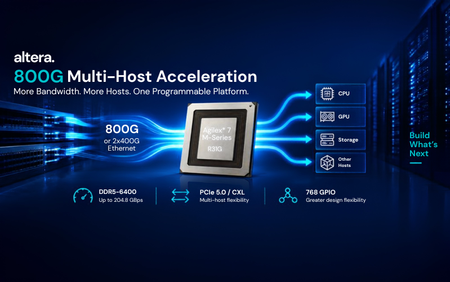
Altera has begun shipping the new Agilex® 7 M-Series R31G multi-host acceleration package, giving customers a new way to build high-bandwidth systems that connect more hosts while moving more data through the network and memory subsystem. R31G is designed for architectures where data must move quickly between the network, memory, and multiple CPUs, GPUs, or other hosts. By bringing 800G or 2x400G Ethernet together with expanded PCIe 5.0/CXL host connectivity, the package opens new possibilities for AI NICs, storage acceleration, cloud acceleration, and other high-throughput platforms. What R31G enables More network bandwidth: 800G or 2x400G Ethernet capability for high-throughput data paths. More host connectivity: Two PCIe 5.0 x16 host interfaces, or up to four independent PCIe 5.0 x8 connections, with CXL support for flexible multi-host architectures. More memory bandwidth and I/O: DDR5-6400 and LPDDR5-6400 support, up to 204.8 GBps of memory bandwidth, and 768 GPIO in a compact 56 x 45 mm package. The result is a programmable platform that can connect, accelerate, and adapt as infrastructure requirements evolve, while keeping high-speed networking, host connectivity, and memory bandwidth tightly integrated. More network bandwidth. More hosts. More memory bandwidth. One programmable platform. Learn more in the Agilex® 7 M-Series product site.
24 days ago0likes
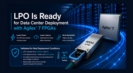
As AI, cloud, and high-performance computing systems continue to scale, data center operators need more bandwidth within increasingly constrained power and thermal envelopes. Linear Pluggable Optics (LPO) offers an important path forward by simplifying optical modules, reducing power consumption, and lowering latency. LPO places signal-conditioning responsibilities in the host device, allowing the optical module to operate without the DSP used in traditional retimed optics. This architecture can reduce optical module power by 30% to 40%, helping data center designers increase connectivity density while simplifying cooling and thermal management. Altera Brings LPO to the FPGA Market Altera is the first FPGA provider to publicly demonstrate Linear Pluggable Optics interoperability using production FPGA devices. Continued validation with LPO modules from Amphenol and FS further demonstrates the breadth of the emerging ecosystem supported by Altera. Agilex® 7 FPGAs and SoCs bring the power and latency advantages of LPO to programmable platforms used in SmartNICs, data processing units, AI accelerators, and custom infrastructure. The initial public demonstration established that Agilex 7 devices could successfully interoperate with 400G LPO modules. The latest validation advances that milestone by confirming that the implementation meets the performance requirements expected for deployment in demanding data center environments. Validated for Real Deployment Conditions Comprehensive testing confirms that Agilex 7 F-Tile transceivers meet the electrical and link-performance requirements defined by the 100G-DR-LPO specification. The validation demonstrated: Compliance with the required transmit, receive, and link-performance criteria Successful interoperability with LPO modules from Amphenol and FS Successful LPO connectivity across distances from 1 meter to 500 meters Consistent performance across temperature and voltage conditions Measurable performance margin beyond required thresholds Testing covered demanding signal conditions, voltage variation, and temperatures ranging from minus 40 degrees Celsius to 105 degrees Celsius for electrical characterization. Functional link testing included a 1-meter LPO connection, a 100-meter active optical cable, and 500-meter LPO modules from Amphenol and FS. The results demonstrate robust, repeatable operation across multiple module suppliers and link distances, with measurable margin relative to the required performance limits. For customers, this validation provides confidence that Agilex® 7 support for LPO is ready for real-world deployment. Following the industry’s first public FPGA interoperability demonstration, the solution has now been evaluated against LPO performance requirements using modules from multiple suppliers and over link distances up to 500 meters. Together, these results demonstrate a practical foundation for deploying LPO connectivity in next-generation data center systems. More Efficient Connectivity for AI and Cloud Infrastructure The value of LPO grows as data centers deploy more high-speed optical connections. Eliminating the DSP from each optical module can reduce power across thousands of links, simplify optical module design, ease thermal pressure at the front panel, and support lower-latency data movement. Agilex 7 FPGAs add programmability to this more efficient optical architecture. Customers can combine LPO connectivity with packet processing, acceleration, security, telemetry, and evolving protocol support on a single adaptable platform. This flexibility is especially valuable for AI clusters and cloud infrastructure, where workloads, network architectures, and connectivity standards continue to evolve. Validation with multiple module vendors also gives system designers greater flexibility as the LPO supplier ecosystem continues to develop. Ready for the Next Generation of Data Centers The combination of public interoperability and comprehensive validation marks a major step for LPO in the FPGA market. Altera has demonstrated that LPO works with production Agilex 7 devices and validated that the solution meets key LPO requirements with measurable operating margin. This gives customers a proven foundation for evaluating and deploying lower-power, lower-latency optical connectivity in real data center environments. With Agilex® 7 FPGAs, LPO is ready for real-world data center deployment.
2 months ago0likes
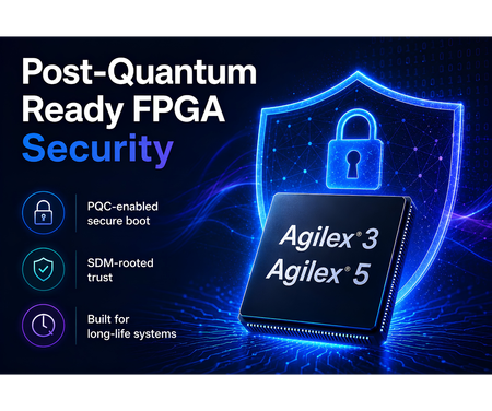
Security requirements are entering a new phase. Systems being designed today may remain deployed for many years, while regulatory expectations, cryptographic standards, and threat models continue to evolve. For designs in industrial, communications, infrastructure, aerospace, defense, and embedded applications, long-term security is becoming a core platform requirement. FPGA-based designs allow designs to meet today’s security needs and evolve with tomorrow’s requirements. Altera is now offering Agilex® 3 and Agilex® 5 devices with PQC-enabled secure boot and configuration support, helping customers prepare for the next generation of security requirements. With the Quartus® Prime Pro Edition 26.1.1 release, customers can begin using a PQC flow that works with Agilex 3 and Agilex 5 based hardware. This milestone extends the security architecture already built into the Agilex platform. Agilex devices use the Secure Device Manager as a hardware root of trust for secure configuration and device management. By combining PQC-capable devices with Quartus software enablement, Altera is helping customers strengthen the FPGA chain of trust as post-quantum requirements move from planning to implementation. The value is immediate and practical. Customers can start designing with supported devices today, while using Quartus 26.1.1 to take advantage of the current software flow. This gives teams a path to address emerging compliance and security expectations without needing a future platform redesign. The same hardware foundation also allows for additional security enhancements over time. Customers designing with PQC-capable Agilex 3 and Agilex 5 devices can benefit from planned software and firmware improvements enabled by the underlying hardware, with no further FPGA hardware upgrade required for those enhancements. Agilex 3 devices bring this capability to power- and cost-optimized FPGA and SoC designs used in embedded, edge, industrial, control, and platform-management applications. Agilex 5 devices extend the same security direction into mid-range FPGA and SoC designs that require higher performance, greater integration, and broader system capability. Post-quantum readiness will continue to advance, and Altera is building that evolution into the Agilex platform roadmap. With PQC-capable Agilex 3 and Agilex 5 devices and Quartus 26.1.1 software enablement, customers have a practical starting point today and a scalable foundation for future security enhancements.
2 months ago0likes