Forum Discussion

GerhardCadek's avatar
GerhardCadek
Icon for New Contributor rankNew Contributor
1 month ago

How-to generate dual-port (read/write) RAM with clock enables

Following Stratix® 10 Embedded Memory User Guide (2025.07.24) chapter 2.11.6 independent clock enables are supported for

  • read/write clock mode
  • input/output clock mode

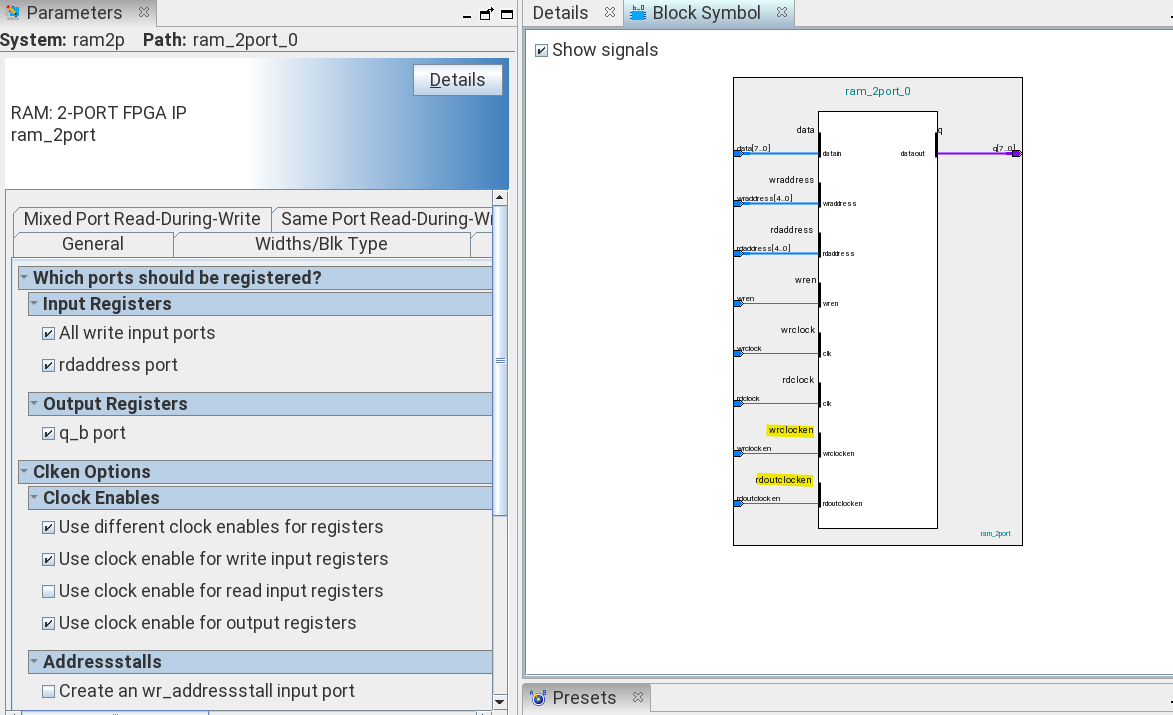
I start a "RAM 2-port" IP generation. I select "one read/write port" in the general tab and "dual clock use separate read and write clock" in the "Clks/Rd,Byte En" tab. Now I enable the clock enables in the "Reg/Clkens/Aclrs" tab "use clock  for read input register" as well as same for "output registers". IP Parameter window immediuately shows an error: 

Error: testram.ram_2port_0: Clock enable for read input registers is unavailable while using 'Dual clock: use separate read and write clocks' for Stratix 10 device family.

This is verified with Quartus Pro 18.1 and 25.3. Is this a bug of the software or the documentation?

17 Replies

  • FvM's avatar
    FvM
    Icon for Super Contributor rankSuper Contributor

    Hi Gerhard,

    I checked some possible RAM configurations with manual setting of clock_enable in direct altera_syncram instantiation, e.g. your above posted setup, but ENA input of PORTBADDR register appeared always unconnected (ENA driver greyed out) in Resource Property Viewer. Output register is in constrast driven by clock_enable1.


    Thus I conclude, the feature isn't actually available for Stratix 10 and Agilex. Another question is if adressstall_b might be used for intended purpose? This would be possible if input clock_enable shall be only applied to address register.

    Regards
    Frank

    P.S.: Same code gives this Resource Property View for Arria 10. ENA input is also driven by clock_enable1. PORTBRE ENA also driven, but shown further down.


  • FvM's avatar
    FvM
    Icon for Super Contributor rankSuper Contributor

    Hi Gerhard,

    thanks for clarification. I didn't clearly understand that Arria 10 still compiles correctly but Agilex 5 and Stratix 10 don't accept the setting. According to Agilex and Stratix 10 Embedded Memory User Guides, this is due to hardware differences, user guide suggests that emulated TDP dual clock mode is necessary to achieve Arria 10 compatible behaviour. Question is if above altera_syncram instantiation actually activates read input and output register clock enable driven by common enable signal.

    To be sure, the behaviour should be verified in a hardware test setup. Simulation model might be partly incorrect.

    Regards Frank

  • Hi Frank,

    yes I'll require both clock enables for read input and read outputs be active which is not available without errors form Stratix10, Agilex5 etc. Its no issue of Quartus Pro versus Quartus Standard. I have these RAMs successfully created for Arria10 using Quartus Pro 18.1 & 23.2.

    This perfectly works as expected. Same settings but different technology (Stratix 10 and newer FPGAs) and I am not able to generate these RAMs

    As mentioned I applied a patch to the generated netlist which at least works in simulation (and is accepted by Quartus during implementation). The DIFF shows the changes:

    Left ist the modified netlist, right the original one generated by Quartus. Basically I "just" changed the CE attributes. I don't know whether this will reliably work in hardware.

    Best regards

    Gerhard

  • FvM's avatar
    FvM
    Icon for Super Contributor rankSuper Contributor

    Hi Gerhard,
    I understand the scenario as follow:
    True dual-port (different clocks), one for read port and one for write port.
    Using clock enable for both ports

    No matter how the clock configuration can be specified in RAM IP GUI, you have essentially one clock enables for  each port. Additionally, address stall (clock enable for address register) can be used, but it's apparently not useful for your application.

    I believe, the correct setting for your configuraton is like this


    You are apparently stumbling upon the requirement of "clock enable for read input registers" and "clock enable for output registers" need either both cleared or set. But that's just the consequence of having a global enable for read port clock.

    RAM IP in Quartus Std. looks different, but has, as far as I'm aware of, same functionality.

    If above configuration doesn't meet your requirements, can you show a screenshot of settings in Quartus Std. RAM IP GUI?

    Regards
    Frank

    • KennyT_altera's avatar
      KennyT_altera
      Icon for Super Contributor rankSuper Contributor

      Hi Gerhard,


      Thank you for your detailed feedback and for sharing your experience across device families and Quartus versions.


      Regarding the clock enable issue for RAM 2-port IP generation on Stratix 10 and Agilex 5: The behavior you observed—where enabling clock enables for read input/output registers is not supported in dual clock mode—is consistent with the hardware architecture differences between Arria 10 and newer device families (Stratix 10/Agilex 5). As noted in the Stratix® 10 Embedded Memory User Guide, independent clock enables are supported for certain modes, but the direct configuration you achieved on Arria 10 is not fully available on Stratix 10 and Agilex 5 due to these hardware changes.


      The Quartus IP GUI restricts these settings to prevent unsupported configurations. While manual netlist modification may work for simulation and, in some cases, implementation, we strongly advise against this for production hardware, as it may not be reliably supported and could lead to unpredictable behavior.

      For true dual-port, dual-clock RAMs requiring independent clock enables on both ports (as in your RX/TX FIFO application), the recommended approach is to use the emulated true dual-port (TDP) mode described in the Stratix 10/Agilex 5 Embedded Memory User Guides. This mode is designed to provide Arria 10-compatible behavior, though it may require some adjustments in your design flow.


      We appreciate your efforts to test and validate in simulation and encourage further hardware testing if you proceed with manual modifications. However, for long-term robustness and supportability, we recommend adhering to Quartus-generated IP configurations and using emulated TDP mode where necessary.


      Thanks

      Best regards,

      Kenny

      • FvM's avatar
        FvM
        Icon for Super Contributor rankSuper Contributor

        Hi Gerhard,

        I found that for the dual-port configuration shown above, rden can be used instead of rdinclockenable. I see same behaviour for all combinations of input and output side enable.

        Regards Frank

  • Hi Frank,
    these RAMs are part of the Ethernet data path to the CPU. The RAMs implement the RX & TX FIFOs. On one side there is the line interface (MAC function) while on the other side there is the CPU interface. Both sides inherently require a different clock. Data on the MAC side is twice the MAC width; thus every other clock the pipeline needs to be hold. On the CPU side the data is transmitted in bursts. After every burst cycle the pipeline again has to be put on hold. This worked perfectly with older technologies until Arria10. Starting with Stratix10 something had been changed in the generation of the RAM. One cannot select the mode as described in the documentation.

    BTW: I modified the generated RAM netlists for both simulation & synthesis. Using these modified netlists the simulation results are OK. Quartus also implements the design without errors. Currently I am trying to find a hardware setup where I can test the implementation of these modified netlists. But I definitely favor a solution without manual patches.

    Regards
    Gerhard

  • FvM's avatar
    FvM
    Icon for Super Contributor rankSuper Contributor

    Hi,

    can you clarify the connection and implemented function of "existing dual-clock RAM with read clock enable"?

    Regards
    Frank

  • Hi Richard,

    Happy New Year to you.

    Due to the holydays and some urgent projects it took a while until I was able to test your suggestion. The brief test result: It does not work.

    I used a simulation (Altera Questa 22.1) of our 10Gbit Ethernet MAC and verified the existing 2-port RAMs dual-clock (Arria 10 with Quartus Standard 20.1.1) with read clock enables against the solution you proposed (Stratix 10 with Quartus Pro 25.3). The FIFO looses using the new RAMs even when using your proposed structure. data. The difference origins out of the fact that obviously just the output register is affected by the "rdoutclocken" while the old "rdclocken" also affected the input side.

    Are there any ideas on that? For me either the documentation is wrong or the Platform Designer is buggy.

    Regards

  • There is the same issue for Agilex 5. Again the documentation states: 

    Independent clock enables are supported in the following clocking modes:• Read/write clock mode—supported for both read and write clocks.• Input/output clock mode—supported for the registers of both ports 


    • RichardT_altera's avatar
      RichardT_altera
      Icon for Super Contributor rankSuper Contributor

      You can use below setting to enable the wrclocken and rdoutclocken.
      - Use different clock enables for registers. (only available on Dual Clock: use separate "read" and "write" clocks)
      - Use clock enable for write input registers.
      - Use clock enable for output registers.


      Regards,
      Richard Tan

      • GerhardCadek's avatar
        GerhardCadek
        Icon for New Contributor rankNew Contributor

        Hi Richard,

        thank you for this tipp. I will try this approach right next week!

        Regards

        Gerhard Cadek