Forum Discussion

Altera_Forum Honored Contributor
9 years agoHonored ContributorConstrained clock appears as unconstrained input
Hello,
I've spent a considerable amount of time several months ago to look into timing constraint issues, but had never understood how it works ... all this staff, despite several manuals I looked through. Then I abandoned it in favour of other things. Recently I returned to that work, and once more face these issues. So here is my constraint file - it was generated by Terasic System Builder and then I added some additional instructions, in particular, create_clock and create_generated_clock. Timing Analysis reports 2 violations: one unconstrained input port and on unconstrained output port. CLOCK_50 No input delay, min/max delays, false-path exceptions, or max skew assignments found. This port has clock assignment. DRAM_CLK No output delay, min/max delays, false-path exceptions, or max skew assignments found. This port has clock assignment. But input port is part of create_clock instruction, so must be considered as constrained, and output port is part of create_generated_clock instruction, so also must be considered as constrained (if my comprehension is correct). Where I've been mistaken ? Thanks in advance.#**************************************************************# This .sdc file is created by Terasic Tool.# Users are recommended to modify this file to match users logic.# **************************************************************
# **************************************************************# Create Clock# **************************************************************
create_clock -period 20.0 -name clk CLOCK_50
create_clock -period 20.0 -name clk_dram# create_clock -period "100 MHz" -name clk_dram
# for enhancing USB BlasterII to be reliable, 25MHz
create_clock -name {altera_reserved_tck} -period 40 {altera_reserved_tck}
set_input_delay -clock altera_reserved_tck -clock_fall 3
set_input_delay -clock altera_reserved_tck -clock_fall 3
set_output_delay -clock altera_reserved_tck 3
# **************************************************************# Create Generated Clock# **************************************************************
create_generated_clock -name clk_sdram_ext -source # derive_pll_clocks
# **************************************************************# Set Clock Latency# *************************************************************
# **************************************************************# Set Clock Uncertainty# **************************************************************
derive_clock_uncertainty
# **************************************************************# Set Input Delay# **************************************************************# Board Delay (Data) + Propagation Delay - Board Delay (Clock)
set_input_delay -max -clock clk_dram -0.048
set_input_delay -min -clock clk_dram -0.057
# **************************************************************# Set Output Delay# **************************************************************# max : Board Delay (Data) - Board Delay (Clock) + tsu (External Device)# min : Board Delay (Data) - Board Delay (Clock) - th (External Device)
set_output_delay -max -clock clk_dram 1.452
set_output_delay -min -clock clk_dram -0.857
set_output_delay -max -clock clk_dram 1.531
set_output_delay -min -clock clk_dram -0.805
set_output_delay -max -clock clk_dram 1.533
set_output_delay -min -clock clk_dram -0.805
set_output_delay -max -clock clk_dram 1.510
set_output_delay -min -clock clk_dram -0.800
set_output_delay -max -clock clk_dram 1.520
set_output_delay -min -clock clk_dram -0.780
set_output_delay -max -clock clk_dram 1.5000
set_output_delay -min -clock clk_dram -0.800
set_output_delay -max -clock clk_dram 1.545
set_output_delay -min -clock clk_dram -0.755
set_output_delay -max -clock clk_dram 1.496
set_output_delay -min -clock clk_dram -0.804
set_output_delay -max -clock clk_dram 1.508
set_output_delay -min -clock clk_dram -0.792
# **************************************************************# Set Clock Groups# **************************************************************
# **************************************************************# Set False Path# **************************************************************
set_false_path -from
set_false_path -from
set_false_path -from * -to
set_false_path -from * -to
19 Replies
 Altera_Forum
Hi,
If I understand you correctly, your PLD receives the reference clock at the CLOCK_50 pin, and internally routes that pin to the DRAM_CLK output pin; all external logic receives its clock from the PLD's DRAM_CLK pin. These changes should fix your warnings:
The first statement defines a logical clock named "clk", which comes from the pin "CLOCK_50". You already had that, but I'm not sure if it really works without "get_ports()", so I added that. The second statement is, as far as I understand it, wrong, so I commented it out. The third statement defines another logical clock, named "clk_dram", which is basically the same as "clk", but measured with pin "DRAM_CLK" as a reference. I fixed the name of the clock that it generates. Below that, there should be all your set_xyz_delay statements, where you already use the clock name "clk_dram". Hope that helps. - GooGooCluster... create_clock -period 20.0 -name clk # create_clock -period 20.0 -name clk_dram ... create_generated_clock -name clk_dram -source ...- Altera_Forum
Thank you GooGooCluster,
I've just tried your suggestions. Unfortunately the result is the same - timing analysis reports two unconstrained ports - clock_50 and dram_clk. --- Quote Start --- If I understand you correctly, your PLD receives the reference clock at the CLOCK_50 pin, and internally routes that pin to the DRAM_CLK output pin; all external logic receives its clock from the PLD's DRAM_CLK pin. --- Quote End --- Yes, the FPGA (Cyclon V) receives 50MHz clock (generated on the board) at clock_50. Then this clock is "redirected" (assign DRAM_CLK = CLOCK_50) to clock external SDRAM chip. Concerning other SDRAM staff (i.e. DRAM_***), all these ports are clocked by the clock, derived from main system clock (i.e. CLOCK_50), as these interface ports are "created" by inserting the "SDRAM controller IP" in Qsys. I used a virtual clock for creating input/output delays for SDRAM staff, which you suggested to comment (i.e.# create_clock -period 20.0 -name clk_dram) because in all manuals that I'v seen until now it's this "mysterious object", named virtual clock, that is used for creating input/output delays. In the same time in all these manuals, the clock for external module is generated outside FPGA, whereas in my case (and I think in majority cases, it's FPGA, that delivers clock for external module). So, I consider your suggestion as quite reasonable, but unfortunately it didn't help ... probably due to some option improperly set somewhere. Regards. - Altera_Forum
I've found the same problem in this thread (April 2012)
http://alterauserforums.net/forum/showthread.php?t=37111&p=153235 ... isn't resolved since 5.5 years !!! - Altera_Forum
Finally I've found the source of problem.
It's caused by assign dram_clk = clock_50 assignment. When I comment it, timing analysis passes without reporting unconstrained input/output. But I still need to "redirect" system clock clock_50 to dram_clk to clock external SDRAM chip. I've tried buf(dram_clk, clock_50) instead of assign dram_clk = clock_50 ... and problem reappeared. Any suggestions ? - Altera_Forum
You should probably use a PLL to generate DRAM_CLK instead of just trying to route it through.
- Altera_Forum
Yes, I know that with PLL it works, but actually I'm trying to do without PLL, as board manufacturer states that at 50MHz no phase shift needed between SDRAM chip clock and SDRAM controller clock.
So is it possible without PLL ? - Altera_Forum
You can set up the PLL compensation mode as a zero delay buffer. That way, it's like the PLL is basically not there.
- Altera_Forum--- Quote Start --- Yes, I know that with PLL it works, but actually I'm trying to do without PLL, as board manufacturer states that at 50MHz no phase shift needed between SDRAM chip clock and SDRAM controller clock. So is it possible without PLL ? --- Quote End --- Yes and no... In one of my designs, I do basically that. I feed a clock into a CPLD, which is used to generate some data, which is then fed to a DAC, together with the clock (from a CPLD I/O pin). It works, but obviously the clock skew inside the CPLD will vary between compilations, even though timing closure is achieved. And I get warnings that what I'm doing is not optimum with regards to jitter. None of that matters for my application; so, yes, it can work, depending on what you want. In another design, I have an FPGA with SDR-SDRAM. Sounds more like your application. That SDRAM is more strict with regards to setup and hold time. In my case, it' was impossible to get timing closure without using a PLL that can fine-tune the clock phase. With another SDRAM controller, another SDRAM chip, another clock frequency, it might have worked without tweaking the phase. However, I have to mention that it practically works with a 180° clock phase (i.e. internally invert the clock, assume routing delay is negligible), even though the timing analyzer complains (I verified the functionality with a FSM that writes PRBS-patterns and reads them back). Why did I use a PLL then? Because that's a commercial product, where I cannot risk that some unit doesn't work because the timings hit the worst-case. In conclusion, I agree with what sstrell wrote. Use a PLL, and use it as a zero-delay buffer. Get your timing constraints to work without warnings. If a timing violation occurs, one option might be to add some phase shift with the PLL instead of doing zero-delay. Uh, well, unless you just want to play with some eval board. Then I personally would be a bit more pragmatic... you mentioned the board manufacturer's recommendation; if you have a way to verify the functionality of the SDRAM, and it just works, I would just call it a day. Sorry for ruining the fun of playing with the timing constraints then... :) But I think we drifted away from the topic a bit, didn't we? The original problem was the SDC file that complained about unconstrained paths...?
- Altera_Forum
I've tried with zero delay buffer: with this option PLL generates an additional output, that should be connected somewhere. I didn't understand this option and finally selected "normal" option.
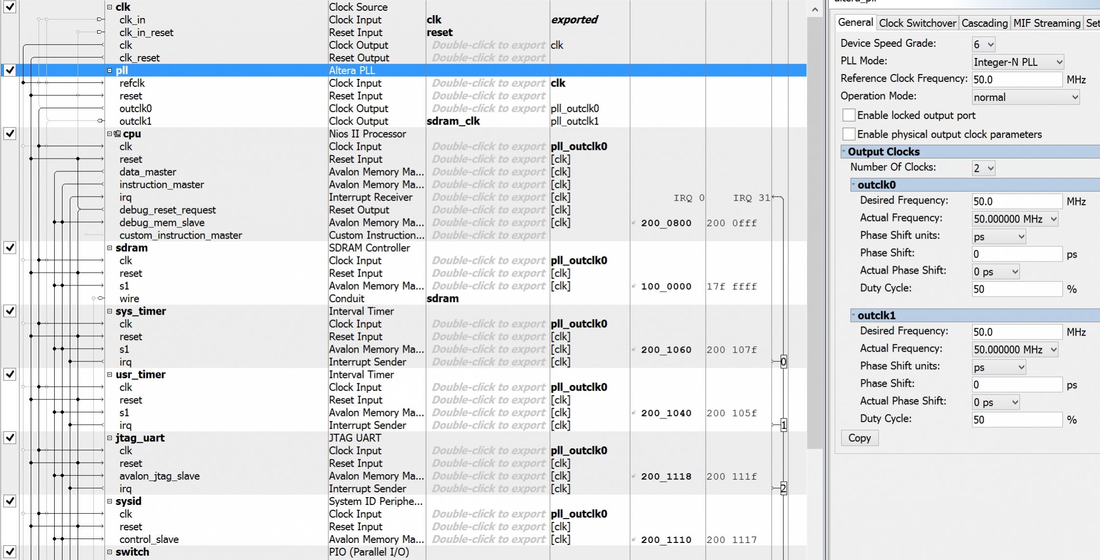
Also I din't increase PLL-generated clocks and didn't introduce phase shift. With this concept the problem didn't completely disappear - while with base clock (i.e. CLOCK_50), it's OK, DRAM_CLK still appears as unconstrained output. Here is fragment of Qsys: https://www.alteraforum.com/forum/attachment.php?attachmentid=14124 And here is .sdc file:
Any comments ?#************************************************************** # This .sdc file is created by Terasic Tool. # Users are recommended to modify this file to match users logic. # ************************************************************** # ************************************************************** # Create Clock # ************************************************************** create_clock -period 20.0 -name clk CLOCK_50 derive_pll_clocks derive_clock_uncertainty # for enhancing USB BlasterII to be reliable, 25MHz create_clock -name {altera_reserved_tck} -period 40 {altera_reserved_tck} set_input_delay -clock altera_reserved_tck -clock_fall 3 set_input_delay -clock altera_reserved_tck -clock_fall 3 set_output_delay -clock altera_reserved_tck 3 # ************************************************************** # Create Generated Clock # ************************************************************** # **** next stetement modified by GooGooCluster *** # create_generated_clock -name clk_dram -source .gpll~PLL_OUTPUT_COUNTER|divclk}] create_generated_clock -name clk_dram -source .gpll~PLL_OUTPUT_COUNTER|divclk}] # ************************************************************** # Set Input Delay # ************************************************************** # Board Delay (Data) + Propagation Delay - Board Delay (Clock) set_input_delay -max -clock clk_dram -0.048 set_input_delay -min -clock clk_dram -0.057 # ************************************************************** # Set Output Delay # ************************************************************** # max : Board Delay (Data) - Board Delay (Clock) + tsu (External Device) # min : Board Delay (Data) - Board Delay (Clock) - th (External Device) set_output_delay -max -clock clk_dram 1.452 set_output_delay -min -clock clk_dram -0.857 set_output_delay -max -clock clk_dram 1.531 set_output_delay -min -clock clk_dram -0.805 set_output_delay -max -clock clk_dram 1.533 set_output_delay -min -clock clk_dram -0.805 set_output_delay -max -clock clk_dram 1.510 set_output_delay -min -clock clk_dram -0.800 set_output_delay -max -clock clk_dram 1.520 set_output_delay -min -clock clk_dram -0.780 set_output_delay -max -clock clk_dram 1.5000 set_output_delay -min -clock clk_dram -0.800 set_output_delay -max -clock clk_dram 1.545 set_output_delay -min -clock clk_dram -0.755 set_output_delay -max -clock clk_dram 1.496 set_output_delay -min -clock clk_dram -0.804 set_output_delay -max -clock clk_dram 1.508 set_output_delay -min -clock clk_dram -0.792 # ************************************************************** # Set Clock Groups # ************************************************************** # ************************************************************** # Set False Path # ************************************************************** set_false_path -from set_false_path -from set_false_path -from * -to set_false_path -from * -to - Altera_Forum
Mysterious !
In very similar design I did before there is no such issues. Short resume: TimeQuest analysis generates unconstrained path error on output dram_clk. This port delivers clock to external SDRAM chip and it's constrained with the following instruction: create_generated_clock -name clk_dram -source [get_pins {u0|pll|altera_pll_i|general[1].gpll~PLL_OUTPUT_COUNTER|divclk}] [get_ports {dram_clk}] Here is TimeQuest diagnostic, related to this DRAM_CLK port (setup analysis): unconstrained output ports: DRAM_CLK No output delay, min/max delays, false-path exceptions, or max skew assignments found. This port has clock assignment. unconstrained output port paths: From To From Clocks u0|pll|altera_pll_i|general[1].gpll~PLL_OUTPUT_COUNTER|divclk DRAM_CLK u0|pll|altera_pll_i|general[0].gpll~FRACTIONAL_PLL|vcoph[0] The same messages are present in hold analysis. Probably I've been mistaken with create_generate_clock instruction ? Thanks.