Forum Discussion

 Occasional Contributor
A design based on the PCIe DMA transfer example design for Arria 10 device.
Hi,
This is a extension of the discussion https://community.intel.com/t5/Programmable-Devices/Modifying-the-PCIe-DMA-transfer-example-design-for-Arria-10/m-p/1484799#M90698 and https://community.intel.com/t5/FPGA-Intellectual-Property/API-calls-failed-while-running-PCIe-DMA-transfer-example-design/m-p/1520494#M28014 where we could not get a solution to the problem we are facing.
We also tried trying to get a Intel Premium help (We are based on a University in USA, but purchased the FPGA and Intel Quartus Prime Pro with normal rate NOT through University reduced rate). But thats is rejected by Intel explaining that since, We are from a University, We are not eligible for Premium help. It would be great if you suggest a way to resolve the issue.
Story in short: We were working on a project to use the FPGA to increase the data throughput in an experiment. We are planning to use FPGA as an intermediate in signal transmission through an optical fiber from electronic readout to the Data Acquisition System. So we need a way to transfer signal though the FPGA (input though the QSFP+ port and output through the PCIe). We were planning to develop a design based on the PCIe DMA transfer example design (that involve the DDR4 memory to store data). In the example design, data is created at a host computer and is written into the DDR4 memory through DMA write through PCIe. And then it read it back to the hot computer to verify the sending data is same as the receiving data.
What we need in our project to stream data from QSFP+ to the DDR4 memory and then DMA read through PCIe to host computer using the API provided.
As an initial step (to test the working of the FIFO + PCIE DMA transfer example design, as our final aim is to get the data from QSFP+ to FIFO to goto the DDR4 element), we used a custom IP of data counter that counts upto 1000 (works on getting an trigger from a switch SW[0] ) to connect to Avalon FIFO IP. Then this design is integrated to the PCIe DMA transfer example design using Platform Builder. The idea is to stream created at the counter though FIFO to the DDR4 memory element. Then DMA read though PCIE to a host computer. But when we try to do DMA read from the host computer, we could not see the counter outputs (which we are suppose to get?).
Great if you could help us out. Any suggestion where to get help for making our design work is highly appreciated.
33 Replies
 VenT_Altera
Frequent Contributor
Hi @Sijith,
Yes, I obtained the .qsys file from the attached ModifiedDesign.zip in the previous thread. May I know have you tried to run the Signal Tap to check the DDR? What is the observation?
The objective of generating the EMIF example design is to observe the connections on how the DDR store the incoming data because your qsys connection seemed off.
Since you have the next step which is using an external source to replace the counter for input data, I'd suggest you to directly go to this step. And then we can debug from there. Because it's not sure if we replace the counter with the external source, it might create other issues or not.
But if you want to use the counter to generate data and stream the data to DDR4 through FIFO, I think the counter should connect to the DDR4.
From the unmodified example design which you've run successfully, it already performed the DMA read and write operations to DDR4.
May I know what is protocol that you used to feed the data stream to FIFO and to DDR?
Thanks.
Best Regards,
VenTing_Intel
 Sijith
Hi,
Thank you very much. Did not finished run SignalTap yet. Will update you very soon the result.
For feeding data from external source, I have to get the design and to develop data transfer design (QSFP+ to the FIFO then to DMA example design) strategy. So thought using counter to test the data transfer from FIFO to DMA transfer example design will be a quick validation I can do first.
In this reply message above (
He was mentioning about the absence of "valid data path from fifo to dma_wr_master ", this need only when we connect the FIFO to DMA, right? Or am I missing something?
The correct way to connect the FIFO to DDR4 is though the EMIF, right?
I have used the Avalon Streaming from counter to FIFO input and Avalon MM from FIFO out to the DDR4.
 FvM
FvMSuper Contributor
Hi,
I didn't realize that you want to buffer counter data in DDR4 memory. But anyway case, it seems that data is send across clock domains without synchronization . Counter and FIFO are running in the PCIe (250 MHz) and DDR4 in the emif_usr_clk domain. I also don't recognize at first sight how DDR4 data path is multiplexed between clock crossing bridge and counter FIFO and how write control for counter is achieved.- VenT_Altera
Hi @Sijith,
Thanks for your update on the Signal Tap progress.
Yes, to connect FIFO to DDR4, it is through EMIF IP as the EMIF IP is used to interface with the memory devices.
Thanks.
Best Regards,
VenTing_Intel
- Sijith
Thank you VenTing,
It would be great if you could have a look to the Platform Designer connections for the modified design to check all connections makes sense for my design purpose (I mentioned earlier) by the time I will update you Signal Tap
- VenT_Altera
Hi @Sijith,
I've looked into your modified design Qsys connection in Platform Designer.
Here are my findings and inquiries:
1. I'd like to ask where do you store the counter value/ source data. From which memory RAM that the Arria 10 Hard IP for PCIe can DMA read from?
As for a normal DMA write operation, the Write Data Mover requires the source address of the data is to be read. The write descriptors table requires the information of:
• Descriptor ID, ranging from 0-127
• Source address
• Destination address
• Size
You may refer to the user guide on the DMA Write operation: https://www.intel.com/content/www/us/en/docs/programmable/683425/18-0/datasheet.html
2. You can connect the FIFO to the EMIF IP to store the source data in the DDR4.
You may refer to the EMIF IP Example Design which I've included the steps to create the Example Design in the previous reply.
There is a clear Qsys connection provided in the Example Design between the data generator (which is Traffic Generator, tg in the Example Design) and EMIF IP for you as a reference when you're trying to connect the data generator to EMIF IP in your design.
3. After you confirm the FIFO to EMIF connection is correct, you may test the DMA read/write. Before that, please check the Signal Tap on the DDR to ensure that the source data generator is correctly stored in the DDR.
If the DMA operation is not working, please check out the PCIe reference design to compare your design with the reference design. In this reference design, there is a clear Qsys connection between the Arria 10 Hard IP for PCIe and the EMIF IP for you to refer to. And, the reference design has DMA transfers. The operation of this reference design shares the same operation as what you wanted to do in your modified design which is to perform DMA read/write from DDR.
Reference Design: https://www.intel.com/content/www/us/en/design-example/714949/intel-arria-10-fpga-pcie-3-0-x8-dma-design-example.html
Reference Design User Guide: https://www.intel.com/content/www/us/en/docs/programmable/683554/18-0/an-829-mm-dma-reference-design.html
Lastly, if you're still failing to get the correct data value from DDR using DMA after following the connections in the above-mentioned Design Example and Reference Design, please send the Signal Tap result to clarify whether the issue is coming from the PCIe to DDR, or counter to DDR. Then, we can continue to debug from there.
I hope the above findings help you proceed with your project.
Thanks.
Best Regards,
VenTing_Intel
- VenT_Altera
- Sijith
Hi VenTing,
Thank you very much. Actually I am facing some issue to get signal tap running. I would like to review you the procedure I followed. Please correct me if i went wrong in some steps or missing something.
1) Opened my counter+fifo+DMA trasfer example design (basically the modified design we were talking about so far) in Quartus Prime Pro.
2)Opened Platform designer and added Signal Tap IP and connected to the design. then validated system integrity and Generated HDL (clicking the GUI tab "Generate HDL") Then compiled the whole design in Quartus prime pro.
3)Opened the Quartus Prime Signal Tap Logical analyser and saved the .stp file. In the Signal Tap GUI, searched for nodes. But could not see any.
Am I missing some step? Do I want add some info in the .stp file manually?
- VenT_Altera
Hi @Sijith,
In order to see the nodes, please ensure that you complete the correct pin assignment in the Pin Planner and compile the project beforehand.
Besides creating a Signal Tap Instance by HDL Instantiation, you can create the Signal Tap instance using the Signal Tap GUI.
Please refer to the steps in Section 2.3.1 to create a Signal Tap instance with the Signal Tap logic analyzer GUI.
User Guide: https://www.intel.com/content/www/us/en/docs/programmable/683819/23-4/faq.html
Thanks.
Best Regards,
VenTing_Intel
- Sijith
Hi VenTing,
Correct pin assignment you meant is for the modified design, right? I have the pin assignment for the modified design (you can see that if you could open the ModifiedDesign file I shared you previously). And I assume I may not need to work on the pin assignment just after adding the Signal Tap IP into the design in the Platform Designer?
I have a pin assignment (as I mentioned above I did not change any pin assignment after adding Signal Tap IP to the design) and did compile it too. But looks something is still missing.
I went through the document and what I could understand is, we can add Signal Tap instances using GUI (So here we dont need to add signal tap IP to the Platform designer system) . Please correct me if I got wrong?
Looking forward for your reply. Thank you.
- VenT_Altera
Hi @Sijith,
Yes, you can run the Signal Tap by creating a Signal Tap instance with the Signal Tap logic analyzer GUI instead of using HDL instantiation (which is through the Signal Tap Logic Analyzer IP).
There are two ways to create a Signal Tap instance in this method:
1. Click Tools ➤ Signal Tap Logic Analyzer.
2. Click File ➤ New ➤ Signal Tap Logic Analyzer File.
You may follow the steps in Section 2.3.1 in the user guide.
Thanks.
Best Regards,
VenTing_Intel
- Sijith
Thank you. I am able to see the nodes. The problem was my version of Quartus Prime Pro (18.1) has the Signal tap GUI with node finder NOT having LIST option instead it has search nodes option. So I hd to search for the needed nodes.
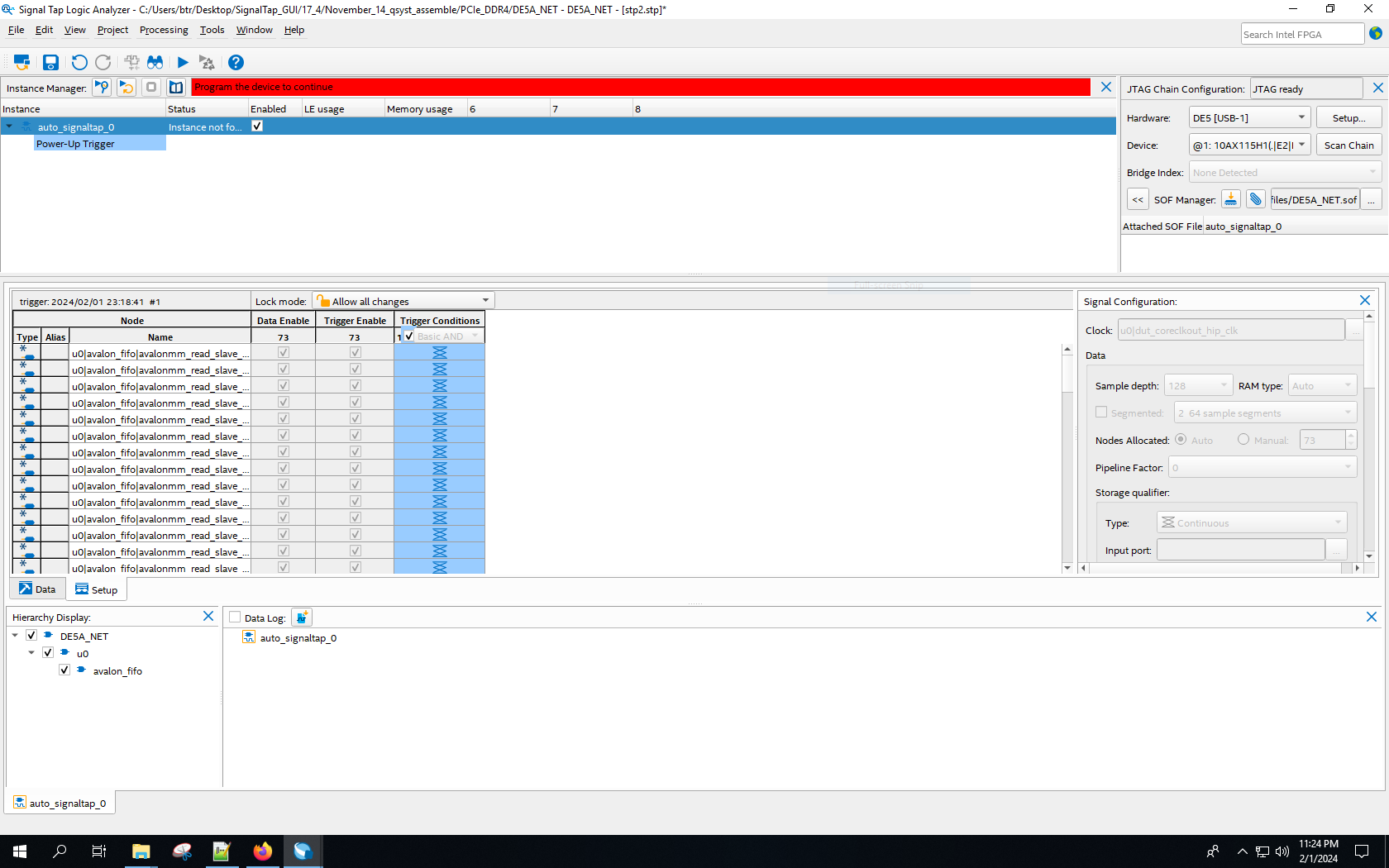
There are still. some problems. After adding nodes to the instance and I could see thee message in Red in the Instance Manager of Signal Tap GUI "Start Rapid Recompile to Continue". But the problem is Rapid Recompile button is inactive as shown in attachment. Then I went for full compilation.
After full compilation and programmed the board through JTAG. But I am getting the message in Instance manager "Program the device to continue". I did it multiple time and again I gets this message. I tried programming using Programmer from the Quartus Prime also (I have seen an intel community thread suggesting to do so https://community.intel.com/t5/Intel-Quartus-Prime-Software/Signal-tap-Program-the-device-to-continue/td-p/1276158 ), but it did not work for me as well. Screenshot attached. I have seen a community thread suggesting to do so.
I have an additional question too. as I am trying to debug the counter fifo outputs at first, can I make an instance having signals that comes to fifo from the counter and from the counter-fifo to the DUT (PCIe DMA) as well? Or I need separate instances for them?
Also, as my design having counter starting when SW[0] =1 (pull up), do I want to set SW[0]=1 after programming the device just before Running the Signal Tap?