Forum Discussion

 New Contributor
Cold Temperature Issue
Hallo,
We used the Agilex5 device in AS configuration connect to external QSPI Flash.
We apply Smart VID interface at the device demands.
When we perform Cold power up at -40C the device is not configured, It seemed the device is not output from the POR, No traffic on the PMBus.
Power sequence and voltage ramp time and levels are OK.
Please advise
Thanks
Asaf
Hi Asaf,
Good to hear that you solved the issue. Yes, all the configuration signals are sensitive can't let the voltage drop even few microseconds.
28 Replies
 Asaf_Bloch
Hello Farabi,
The 3.3V ramping because there are pull-up resistors connected to the system 3.3V, it is low voltage level,
Anyway I moved it and it did not change the cold issue.
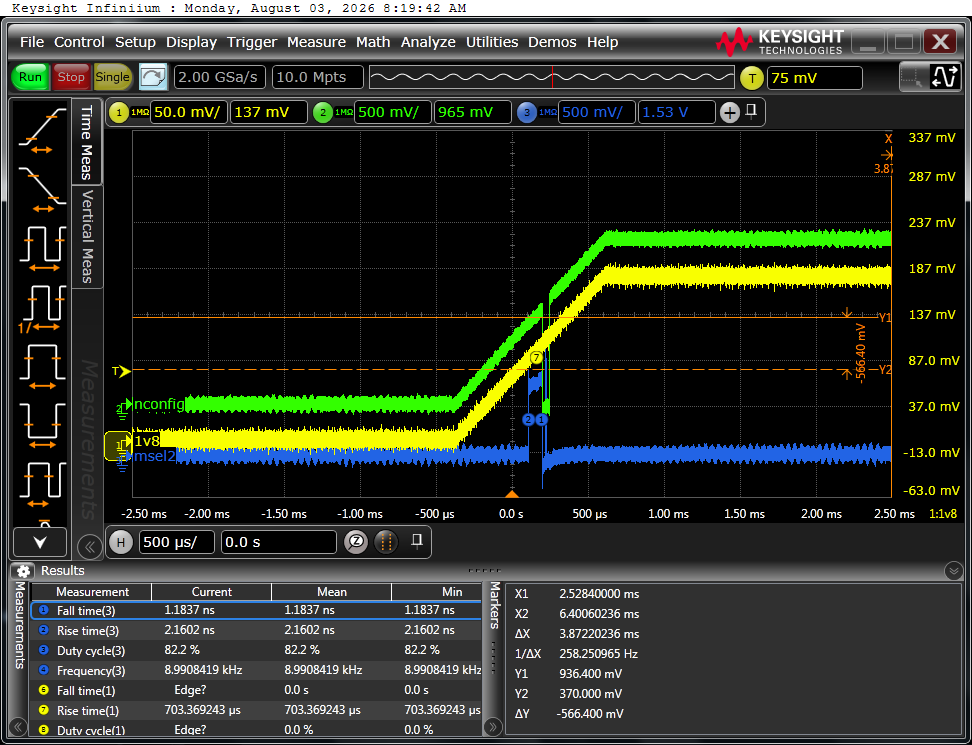
I notice the MSEL and nconfige signals are pull up and down during Vccio_SDM ramping, is it normal behavior? See attached
Thanks
Asaf
 Farabi_Altera
Regular Contributor
HI Asaf,
No that is not normal. MSEL is a fixed connection either HIGH or LOW only. It should not toggle during configuration.
Please connect MSEL pin directly to VCC for HIGH, and directly to GND for LOW setup. Dont control the MSEL.
regards,
Farabi
- Asaf_Bloch
Thanks Farabi,
The issue is after configuration I see the MSE2 is rising to 1.8V, seemed it by the FPAG, is it normal?
Can it harm the pin?
Thanks
Asaf
 dpcsu_e
Hi,
just a short question (do not want to deter this thread): how did you detect it is not out of POR?
(maybe relevant maybe not) On 2 out of 50 Agilex3 devices we have met with similar issue and resulted that over JTAG idcode was read as F36FF0DD instead of 4365B0DD. Is it equivalent to this same issue that SDM ROM code is not coming out of POR? do you observe similar behavior?
How does your power topology looks like?
We have 1.8V and 3.3V HVIO and if 3.3V HVIO's VCCIO do not get some minor accidental backfeed which raises it to 0.6V then FPGA stays in POR.
Voltage rail sequence is 0.75V -> 1.8V -> 1.2V -> 3.3V.
Is it ok to bring up 1.8V SDM and 1.8V VCCIO at the same time or should we bring up the 1.8V+3.3V VCCIO after 1.2V?
Thanks,
Peter- Asaf_Bloch
Hi dpcsu,
Thanks for your reply
Our voltage rail sequence is VID, 08V -> 1.8V -> 1.2V, 3.3 VCCIO
We detect the POR issue because we don't see any signal transitions after power up (nStatus, PMBus), JTAG detect the device.
How did you read the SDM ROM?
Any way we repeat the test with other PCB and it pass successfully, so we examine if it specific PCB issue.
regards
Asaf
- Farabi_Altera
Hello Asaf, Peter,
Do you have update?
regards,
Farabi
- Farabi_Altera
Hello,
Can you share below information:
1- QSPI flash part number
2- VR(Voltage regulator) part number
3- Agilex5 part number
regards,
Farabi
- Asaf_Bloch
Hello Farabi,
1 - QSPI Flash - MT25QU256ABA8E12-1SIT by Micron
2 - VR - LT7184SRV#TRPBF by Analog Device
3 - Agilex5 - A5EC043AB23AI2E
Thanks
Asaf
- Farabi_Altera
Hello Asaf,
If the device is not output from POR, do you have the oscilloscope capture the power rails ramping up?
Any abnormal voltage ramp up during power up? Especially all the power rails monitored by POR circuitry.
regards,
Farabi