Altera_Forum Honored Contributor
16 years agoHonored ContributorAsynchronous adress decoder
Hi,
I have heired an old design which contains of a lot of AHDL moduls. I would like to rewrite these moduls into VHDL so that I can simulate them in modelsim. One thing I realized is that the AHDL file used some kind of asynchronous adress decoding. this means that if the module is connected to the Avalon bus (as custom component or as an "Interface to user logic" like in my case) there are no wait timings. This means that the adress is given by the master on the first clock cycle and the slave has readily brought up the data at the second clock cycle. This can be done in AHDL like this:CASE ADR IS
WHEN 0 => Q = counter1.q;
WHEN 1 => Q = counter2.q;
WHEN 2 => Q = counter3.q;
END CASE;process(adr)
begin
case adr is
when b"00" => q <= ('0' & '0' &'0' &'0' &'0' &'0' &'0' &'0' & counter1);
when b"01" => q <= ('0' & '0' &'0' &'0' &'0' &'0' &'0' &'0' & counter2);
when b"10" => q <= counter3;
when others => q <= (others => '0');
end case;
end process;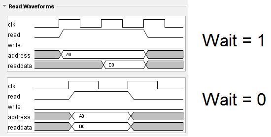