Forum Discussion

 New Contributor
Aria V Display Port core sometimes disconnected
Hi All
We have a PCB board we designed with AMD 8860 GPU that sends DP video to Aria V Display Port core (Qsys). In some of our boards we sometimes have DP connection issues.
The video signal goes to altera_xcvr_native_av and when RX is out of lock we see multiple retries on the DP AUX channel.
We came across this bug:
in our case the enable GPU is not checked.
Can anyone confirm this issue is also applicable to Aria V Display Port?
Thanks
Ariel
50 Replies
 Deshi_Intel
Regular Contributor
Hi,
Transceiver architecture design is different from one FPGA family to another. So, not recommended for you to switch to other FPGA product as well.
It's preferable to stick with AV example design to debug either on your custom board or using the AV starter kit board.
For AV starter kit board debug :
- No, we don't have good way to isolate whether it is dev kit board or Bitec daughter card issue. You can check with whoever person that passed you these board to figure out whether the board is still healthy or any special board rework is done in the past or not
- Your latest NIOS II screenshot showing somehow the initialization is not completed and seems stuck.
- Have you tried to toggle the resetn pin control via pressing push button switch 4 ?
- Or reprogram NIOS II elf file again to see if it helps ?
- Other thing that you can check on the dev kit is launch the clock controller GUI software that comes with dev kit installer software to verify you are outputing the correct clock frequency to AV DP example design
For your own AV custom board debug :
- This is another debug direction also since our original debug goal is to verify your board SI issue via MSA log dump
- We wanted to bring up NIOS II to dump MSA log and you have successfully done it on AV started kit board
- Can you revisit your own board to bring up NIOS II and dump MSA log with "modified AV example design that match your board connection" ? This will be more meaningful than spent time to debug AV starter kit board
Thanks.
Regards,
dlim
- Deshi_Intel
Hi,
Next let's discuss about your MSA log file
- May I know this MSA log file is result output from AV starter kit board or your own custom board ? I presume it's AV starter kit board result ?
- From the MSA log file, you can see that the BER rate is pretty bad for all lanes.
- If you are using AV starter kit board then byright your board signal integrity is good. It shouldn't be that bad unless there is some issue with your board or the Bitec daughter card itself
- Ensure the Bitec daughter card is tightly connect to the board and the AV starter kit board is set with all default switch setting
- Else you can also try with the sof file that I attached in previous post
- You can also change DP cable or switch to test out other GPU since you already have golden ref design and board.
- Pls try out lower video resolution as well
- Another option is to change DP IP bit per colour (bpc) setting to either 8 to 10 to try out
- Else if the MSA log is from your own custom board then you know that your board SI is pretty bad
- Then you will need to review your board SI issue accordingly
Thanks.
Regards,
dlim
 relsaar
Hi,
In my priveouse post I was referring to the av_sk_4k.
I programed the sof file you sent and got the same results:
LEDs in on state: D21, D22, D23, D24, D12, D15
LED D20 - is bilnking
LCD show message "Not Connected"
Cable were tested OK from my PC to the monitor, all the av sk SW setting are default and similar to page 18#.
Checked with alternative GPU and also with 800X600 resolusion and with color depth =8 bit and it still looks similar.
Bitec daughter displayport card is tightly secured to the AV SK with screws.when I'm not loading the NIOS (as you suggested) I can't get the MSA LOG - please see attached terminal capture.
=Can I assume there is a failure in the hardware?
Please advise how can we tell if the failure is on the Arria V SK or at the Bitec daughter displayport card?
thanks
Ariel Saar
- relsaar
Hi
I can see that the Bitec Displayport can also be Compatibility with:
•Cyclone V
•Arria II and V
•Stratix I, IV and Vwe should also have Stratix IV and I get other evaluation kits as a loan - do you have an example design sof file for all of those cards?
Thanks
Ariel
- Deshi_Intel
Hi,
It's good to know that you have AV dev kit board and Bitec DP daughter card to port over the DP example design.
Yet I noticed you are not using AV starter kit board that matched with AV example design pinout setting.
- That means you need to manually check the pin connection on your AV board and modify the example design pin setting accordingly.
From your NIOS II terminal screenshot, I can see the "Started ..." print out which means NIOS II is already running. You just need to press wither "s" button or the user_pb[0] button to dump MSA log
- If it doesn't work and nothing happen then I suspect could be due to wrong clock frequency to NIOS or user_pb[0] pin assignment is not done correctly
- In short, pls ensure all the DP connection, IO standard, clock frequency, reset control and user_pb[0] setting is being taken care of to match with your AV board design
From my side, I will check next week to see if I can find AV started kit board in office to program the example design and show you screenshot of MSA dump. (I am now working from home due to Covid 19 control restriction in my country. We required permission to go back office)
Thanks for your understanding
Regards,
dlim
- relsaar
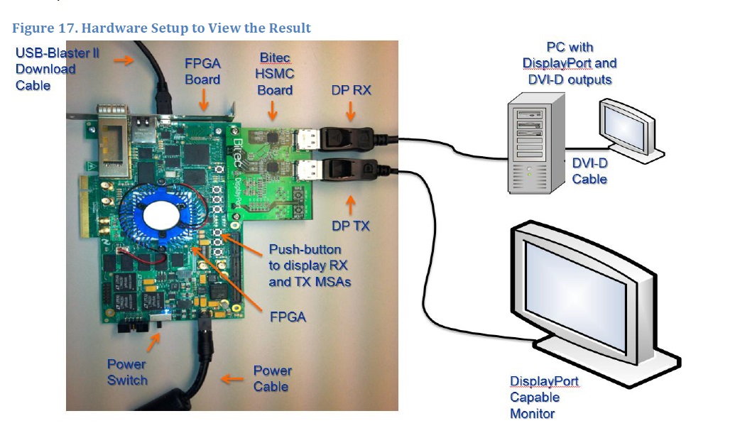
Hi,
I'm sorry - the setup photo I sent was taking from DisplayPort_RX_and_TX_Desgin_Example_AN_r1.pdf page 41#, my board is the Arria V starter KIT (see photo). I checked the pinout of a few signal in the project pin planner vs the schematics of my board and verify it matches. Then I recompile av_sk_4k project an this time I managed to get the log output (see MSA_LOG.txt) but there is no image on the TX and RX is not detected on my PC as a secondary screen.
looking on the Bitec Display Port Daughter Card schematics and A5GX_STARTER_C.pdf schematics – it looks like the HSMA_TX_P4 to HSMA_TX_P0 was cross routed (e.g 4# goes to 0#) I changed that but got the same results.
then I checked the PLL of my design example vs the above PDF and see some gaps.
according to the pdf the top module is not top.v but sv_dp_demo.v and it looks very different from the top level entity I found at altera\15.0\ip\altera\altera_dp\hw_demo\av_sk_4k. (see image SV_DP_DEMO-Top module.jpg can be found at the pdf on page 3#)from the above PDF link - it looks like this Bitec Display Port Daughter Card was tested with a different example design.
Also I discovered that our design was based on this sv_dp_demo.v entity and not the top.v.I managed to find this sv_dp_demo.v design example and tried to test it on the same setup but unfortunately the elf was failed to load.
I tried to migrate this project to Quartos 15.0 but the IP upgrade was failed (see attached log)Please advise how can I proceed.
Thanks
Ariel
- Deshi_Intel
Hi,
You probably miss out my earlier AV DP example design explanation.
- Pls don't refer to other DP example design link else it will create extra confusion to you.
For AV DP example design :
- You should just use the av_sk_4k example design that I shared with you
- The example design doc explanation is available in DP user guide doc chapter 4
You do not need to change anything on this example design if you are already using AV starter kit board + Bitec HMSC rev 11 DP daughter card
- Just compile original av_sk_4k design (unchanged), program the sof file. That's all. NIOS ELF file download is not required.
- Anyway, attached is the AV example design sof file for your reference again
- Make sure you use "factory default switch setting" following AV starter kit user guide doc (page 18)
- https://www.intel.com/content/dam/www/programmable/us/en/pdfs/literature/ug/ug_avgx_starter_dev_kit.pdf
Thanks.
Regards,
dlim
- Deshi_Intel
Let's try your best to bring up NIOS II connection first so that we can dump MSA log
- Deshi_Intel
Hi,
Ya, you shouldn't change NIOS II address location in your design.
- If you modify the address in QSYS then you just need to change it back
- Else if you modify the c code design then you can run "build_sw.sh" script in example design to rebuild the NIOS II software and regenerate the new ELF file again.
- Whenever you touch on the design in software folder, remember to always rebuild software to generate updated elf file, then download and program ELF file again. Else you can also recompile while Quartus project to integrate ELF file design into sof file
- You can learn more about the example design in DP user guide chapter 4
Aux channel is a must for DP link training and policy maker communication update.
- Anyhow, Aux channel is just running at very low speed - 1MHz or 16MHz like that. There shouldn't be signal integrity concern but I do worry whether the Aux channel board design connection is done correctly or not.
- I found out DP board design guideline doc (AN745, page 9 onwards that talks about Aux channel design). You can want to check it out as well
Thanks.
Regards,
dlim
- Deshi_Intel
Additional note - you may want to cross check to ensure example design QSYS NIOS II clock and reset is supplied correctly.
Thanks.
- relsaar
Hi,
I tried to download the NIOS 2 elf file and got an error (see attached).
then I checked the address of the example design Vs my modified example design and realized the address were changed during the modification process.
I think this is the root cause for NIOS load failure - I'll try to change back the address but if it will faile I'll need to create a new elf - can you please address me to suitable userguide?
by the way I'd like to verify if the AUX signal integrity is cauing the MSA drop, is there any option to redundent the AUX channel in the DP setup GUI?
thanks
Ariel
- Deshi_Intel
Hi,
What I meant on watch out on all the clock frequency that you supply to DP design is
- You have modified DP Sink IP data rate and pixel output mode setting, then I would expect you need to modify the clock frequency supplied to example design accordingly like (DP video clock, NativePHY frequency setting, IOPLL setting and etc accordingly) Else pls revert the setting back and keep the changes min
- DP aux channel carry important debug info so you shouldn't remove it. Since you mentioned it's working on your original DP design then you just need to modify the example design
- You can learn more about the DP example design in Intel DP user guide chapter 4
For MSA log dump debug :
- Below AN793 (page 20) show you screen shot of MSA log dump example
- https://www.intel.com/content/dam/www/programmable/us/en/pdfs/literature/an/an793.pdf
- Just wonder after you press "S" and there is no respond from NIOS II terminal ?
- Another method to trigger MSA log dump is via triggering "user_pb[0]" signal port in DP example design
- If both method also failed then you may want to double check whether your NIOS II is initiated correctly ? From AN793 screen shot, I can see some green wording in NIOS II terminal showing connection setup to NIOS II CPU
- You can also try to reprogram the NIOS II elf file again in NIOS II command shell using below command, then repeat the MSA log dump procedure
- nios2-download dp_demo.elf
- The elf file is located in \av_sk_4k_v15_0\software\dp_demo\
Thanks.
Regards,
dlim
- Deshi_Intel
Hi,
There are a lot of design changes that you made. It's hard for me to comment whether everything is done correctly or not.
- The goal is we want to stay as close as to original example design with min changes
- I noticed you changes the DP Rx link rate and pixel output mode.
- Actually it's fine to stay with default setting due to you are using example design and you don't need to worry about the clock frequency changes. DP link training will just down train from 5.4G to 1.62G
- But now you need to watch out on all the clock frequency that you supply to DP design.
- Pls revert back to match original DP example design if you still encounter failure in hardware testing later
Regarding the MSA log dump
- Sorry, my bad. I miss out one step.
- In NIOSII shell terminal, type nios2-terminal to enter NIOS console first
- Then press "s" to print MSA log
Thanks.
Regards,
dlim
- relsaar
Hi,
all of the changes I made to the example design were mandatory:
1. we have no 100M clock available on the board so I had to generate one with current PLL also our DP ref clock is derived from 162MHz so I had to change it as well.
2. the DP Aux channel should be Bidirectional and since our board has no such external IC I had to add it to the example design (unless the Aux channel can be entirely removed some how??)
3. our board has only one lane of Rx DP so I cancel all other lanes - I can add it back but I see no point.
I can revert back to 5.4G if you think it may help.
I'm not sure what did you mean by:
- But now you need to watch out on all the clock frequency that you supply to DP design.
Please explain
I tried to get a BER report from the NIOS command shell by typing nios2-terminal as you suggested but then the command line was locked to further typing (please see attached image) I verify the USB bluster is detected properly in the device manager (please see attached image)
Please advise how can we proceed?
Thanks
Ariel
- relsaar
Hi,
I got some assistent from a local SW FAE on how to properly load the NIOS2 processor, however it did not work out on our boards.
So I managed to get an Arria V evaluation board and a bitech doughter display port extender . I connected the evaluation board Rx to my docking display port output and the evaluation board Tx to my monitor(see photo).
When power up the board my windows 10 detect a new monitor on the display settings and during the SOF and .ELF load I got file transfer positive feedback (those werethe genuin files from the example design), however after I type: NIOS2-terminal I got no response and S or s command are not recognized then the new monitor detection was disappear. I also opened a secondary NIOS2 command shell to read NIOS messages but noting was printed. (see shell print capture)
Please advise how can we proceed?
Thanks
Ariel Saar
- Deshi_Intel
Hi,
Don't use quartus_sh command to execute runall.tcl script in NIOS II terminal
Use below command instead then it should works.
- source runall.tcl
Let me know if you still face issue in generating the example design then I will generate and share it with you via Intel FTP server. The example design file size is quite big (~300MB). Hence, can't be shared as file attachment in this forum community.
I won't recommend to jump into debugging board SI issue until we verify it using MSA log from DP example design.
- Anyway, feel free to learn more about transceiver toolkit info in below link
- https://www.intel.com/content/www/us/en/programmable/products/design-software/fpga-design/quartus-prime/features/swf-transceiver-toolkit.html
- You can download toolkit example design and also easily google for transceiver toolkit short youtube video to get a feel on how it works. You can only verify the data integrity using PRBS generator/checker build in FPGA transceiver channel but don't expect to see fancy eye diagram from toolkit
Thanks.
Regards,
dlim
- relsaar
Hi dlim
I managed to create and compile successfully the example project. since my PCB has only one lane of DP Rx I had to make some changes and customize the example design. attached are updated top.v, pinout table and Qsys GUI settings.
Also since we don't have an external Bidirectional buffer on the board I added "arriav_io_ibuf" internally (see aux_buf_iobuf_bidir_nho_i at top.v) - in my legacy design we also used Bidirectional buffer on those signals.
Finally I created a SignalTap with some signals to verify if the example design gets any input video signal.
The design was compiled without any errors but it looks like the display port Rx does not receive any signal since there is no MSA lock (only occasional negative pulses on Rx Aux In - see attached image)
when I program my legacy design I get steady msa lock most of the time and I'm using the same application to configure the GPU to generate same DP signal. Can you please help me find out what is wrong?
- did I forget any important pin assignment or pinout?
- did I change any settings that disrupted the design to receive DP?
Please let me know if you need more data.
Thanks
Ariel
- relsaar
- Deshi_Intel
Hi,
- Regarding Quartus timequest report.
- You shouldn't need to run additional timing analysis. By default. once you compile your design with STA optional enable. You should be able to view the Timequest compilation summary. Do you see any red wording highlight in compilation summary indicating timing violation in your design ?
- Your DP video bandwidth is sufficient.
- Ya, your error signal toggling looks weird. Let's use MSA log dump from Intel FPGA DP example design to better confirm your BER number. DP IP internally has coded some BER threshold value, once error assertion hit the threshold limit then MSA lock will be de-asserted
Below is the steps to generate MSA log file
- Locate AV DP example design in your Quartus installation folder. Example path below
- C:\intelFPGA\16.1\ip\altera\altera_dp\hw_demo\av_sk_4k
- Execute runall.tcl script in NIOS II shell terminal to generate and compile example design
- Modify the example design FPGA device OPN and pinout to match with your board then compile design again
- Program the DP example design sof file to your board
- Launch NIOS II shell terminal again, press "s" to capture MSA log file
Share with me the MSA log file for both passing board and failing board then we can further analyze your failure issue.
Thanks.
Regards,
dlim
- relsaar
Hi
I opened the NIOS II shell terminal and navegated example design location then I executed the tcl:
Ariel@Ariel /cygdrive/d/altera/15.0/ip/altera/altera_dp/hw_demo/av_sk_4k
$ quartus_sh -t runall.tclthen I got:
Info: *******************************************************************
Info: Running Quartus II 64-Bit Shell
Info: Version 15.0.0 Build 145 04/22/2015 SJ Full Version
Info: Copyright (C) 1991-2015 Altera Corporation. All rights reserved.
Info: Your use of Altera Corporation's design tools, logic functions
Info: and other software and tools, and its AMPP partner logic
Info: functions, and any output files from any of the foregoing
Info: (including device programming or simulation files), and any
Info: associated documentation or information are expressly subject
Info: to the terms and conditions of the Altera Program License
Info: Subscription Agreement, the Altera Quartus II License Agreement,
Info: the Altera MegaCore Function License Agreement, or other
Info: applicable license agreement, including, without limitation,
Info: that your use is for the sole purpose of programming logic
Info: devices manufactured by Altera and sold by Altera or its
Info: authorized distributors. Please refer to the applicable
Info: agreement for further details.
Info: Processing started: Tue Jan 05 13:02:26 2021
Info: Command: quartus_sh -t runall.tcl
------------------------------------------------
can't read "QUARTUS_ROOTDIR": no such variable
while executing
"export PATH=`cygpath -u $QUARTUS_ROOTDIR/bin64`:$PATH"
(file "runall.tcl" line 24)
------------------------------------------------
Error (23031): Evaluation of Tcl script runall.tcl unsuccessful
Error: Quartus II 64-Bit Shell was unsuccessful. 1 error, 0 warnings
Error: Peak virtual memory: 4361 megabytes
Error: Processing ended: Tue Jan 05 13:02:28 2021
Error: Elapsed time: 00:00:02
Error: Total CPU time (on all processors): 00:00:01I added my path : %QUARTUS_ROOTDIR%\bin64 but was not helpful. Also tried to open an empty project add the content of av_sk_4k and run it from tools -> Tcl scripts , but it failed as well.
any idea how to proceed?
Please advise if I can run system console Transceiver toolkit to sample the display port "eye" and derive the signal quality from it? it it' s applicable please refers me suitable user guide or send instructions.
Thanks
Ariel