Altera_Forum Honored Contributor
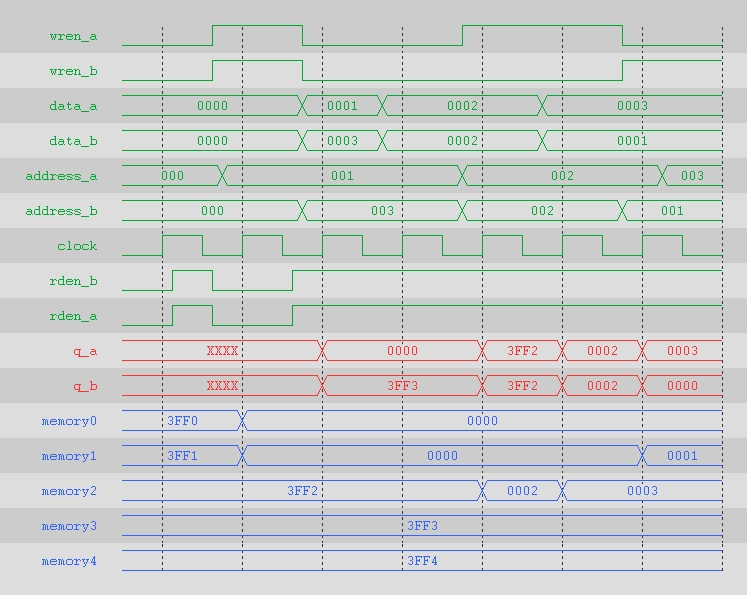
16 years agoHonored ContributorIP AltsyncRam -- Read/Write operations issue
Hi all,
I have another issue using the RAM IP core generated with the MegaFunction wizard. Here's the entity of my RAM and its instanciation:
GENERIC(
ADDRESS_WIDTH : IN INTEGER ;
PIXEL_WIDTH : IN INTEGER

);
PORT
(
address_a : IN STD_LOGIC_VECTOR (ADDRESS_WIDTH-1 DOWNTO 0);
address_b : IN STD_LOGIC_VECTOR (ADDRESS_WIDTH-1 DOWNTO 0);
addressstall_a : IN STD_LOGIC;
addressstall_b : IN STD_LOGIC;
clock : IN STD_LOGIC ;
data_a : IN STD_LOGIC_VECTOR (PIXEL_WIDTH-1 DOWNTO 0);
data_b : IN STD_LOGIC_VECTOR (PIXEL_WIDTH-1 DOWNTO 0);
rden_a : IN STD_LOGIC := '1';
rden_b : IN STD_LOGIC := '1';
wren_a : IN STD_LOGIC := '1';
wren_b : IN STD_LOGIC := '1';
q_a : OUT STD_LOGIC_VECTOR (PIXEL_WIDTH-1 DOWNTO 0);
q_b : OUT STD_LOGIC_VECTOR (PIXEL_WIDTH-1 DOWNTO 0)
);
altsyncram_component : altsyncram
GENERIC MAP (
address_reg_b => "CLOCK0",
clock_enable_input_a => "BYPASS",
clock_enable_input_b => "BYPASS",
clock_enable_output_a => "BYPASS",
clock_enable_output_b => "BYPASS",
indata_reg_b => "CLOCK0",
intended_device_family => "Cyclone III",
lpm_type => "altsyncram",
numwords_a => 2**ADDRESS_WIDTH,
numwords_b => 2**ADDRESS_WIDTH,
operation_mode => "BIDIR_DUAL_PORT",
outdata_aclr_a => "NONE",
outdata_aclr_b => "NONE",
outdata_reg_a => "UNREGISTERED",
outdata_reg_b => "UNREGISTERED",
power_up_uninitialized => "FALSE",
read_during_write_mode_mixed_ports => "OLD_DATA",--OLD_DATA
read_during_write_mode_port_a => "OLD_DATA",
read_during_write_mode_port_b => "OLD_DATA",
widthad_a => ADDRESS_WIDTH,
widthad_b => ADDRESS_WIDTH,
width_a => PIXEL_WIDTH,
width_b => PIXEL_WIDTH,
width_byteena_a => 4,
width_byteena_b => 4,
wrcontrol_wraddress_reg_b => "CLOCK0",
width_b => PIXEL_WIDTH,
width_byteena_a => 4,
width_byteena_b => 4,
wrcontrol_wraddress_reg_b => "CLOCK0"