Forum Discussion

xiaohao's avatar
xiaohao
Icon for New Contributor rankNew Contributor
16 days ago

agilex 7 Platform Designer PIO addr width

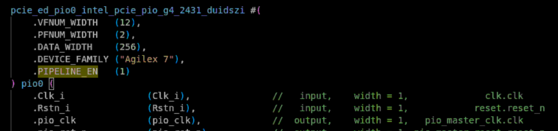
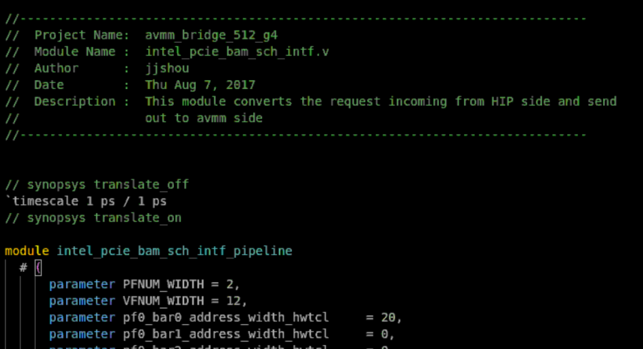
I am using the PIO example design of the P-Tile AVST PCIe IP on Intel Agilex 7. The original design maps a 16KB RAM to BAR0. Since my design requires a larger address space, I modified the PCIe IP's BAR configuration to increase BAR0 size to 2MB. However, I soon discovered that in the "PIO Design Example for PCI Express Gen4," the module converting AVST to AVMM only supports a 16KB address space after conversion. I then replaced it with the "PCIe PIO" IP core, but found that it can only access a 1MB region. What should I do?


6 Replies

  • xiaohao's avatar
    xiaohao
    Icon for New Contributor rankNew Contributor

    I am aware that the example project uses the "PIO Design Example for PCI Express Gen4" module, which defaults to a 16 KB address range mapping. Therefore, I have switched to using the PCIe PIO module.

    I have identified the root cause of the issue and verified that the modification is effective. In the code generated by PIO, certain default macro parameters restrict the accessible memory region to only 1 MB under default configuration. I believe this is an issue with the IP core, as it may mislead or confuse users unfamiliar with this detail (the PIO module only allows configuration of the data access width; however, with the default address range set to 64-bit, the effective accessible address range is limited to merely 1 MB).  

    Additionally, is there any official documentation available specifically for this PIO module?


    This mask prevents me from accessing a larger address range.

    Thank you very much for your suggestions. Regarding the DMA-related content, I haven't implemented it yet (including the PCIe AVST DMA example project). If I want to use DMA to access the on-chip RAM, which example project would be more suitable: PCIe AVST DMA or PCIe Multichannel DMA?

  • After you expand the BAR0 size, you'll need to expand some related modules inside PCIe PIO as well if you really need 2M size. if you'd like to check, a performance design like DMA doesn't always require a large BAR0. The way to use on-chip ram is important.


    Since the PIO module does the AVST to AVMM transformation, here are some places I think you can try. Below filenames could be different from yours.


    After the completion of Synthesis, you can find below module in ip/pcie_ed/pcie_ed_pio0/synth/pcie_ed_pio.v.

    You may increase the PIPELINE_EN to a larger number.


    This file ip/pcie_ed/intel_pcie_pio_g4_2431/synth/intel_pcie_bam_sch_intf_pipeline.sv does HIP to AVMM conversion. 


    Right there, you can find a 16KB FIFO here. I think you need to expand both read and write FIFOs for a larger amount of data.


    Regards,

    Rong


  • Hi,


    AVMM is no longer used in PCIe example designs. If you still want to use PCIe+AVMM, you can upgrade your original design to a newer Quartus. 


    If you want to try PCIe+AVST and have problem in using the BAR0, please let me know your Quartus version.


    Regards,

    Rong


    • xiaohao's avatar
      xiaohao
      Icon for New Contributor rankNew Contributor

      I am using Quartus 24.1. I believe I may not have expressed myself clearly earlier: I am not using a PCIe IP with an AVMM interface; rather, I am accessing the RAM directly via PIO. The core of my issue lies in the intermediate PIO conversion module, which has a constrained address range. For example, when performing a read or write operation to address 0x1FFFF0, the address is altered to 0x0FFFF0 after passing through the PIO module.

      • RongY_altera's avatar
        RongY_altera
        Icon for Contributor rankContributor

        Thanks. Now I understand.


        Can you share me the output of lspci?


        Regards,

        Rong