Forum Discussion

 Honored Contributor
Gated transceiver operation on Transceiver SI Development Kit Stratix V GX board
Hi,
I have been trying to use the transceivers on the Transceiver SI Development Kit Stratix V GX board and managed to successfully use them in continuous mode. However I would like to be able to make them work in a gated mode where bits will be sent only during specific interval. I have implemented a binary counter which I would like to use as a reference for gating the output data. The operation that I want to implement is basically to have as an output a signal that is a result of an AND operation between the 10G continuous data and the binary counter (~400ns period). I have tried by using the reset signal, but that apparently messes up with the transceiver. I have tried to play with the assignments and allocate the output to two different transceivers (1:2 demultiplexing) but I always get some physical limitations warnings and the fitter doesn't compile successfully. If someone has a suggestion on how to implement this or has already done it, I would appreciate your help :) I have instantiated two .qsys systems, one as a 10G clock for triggering purposes and another one as a data channel. The top level file is the a2ch_TDM_clock.v file which I adapted from the transceiver examples.14 Replies
 Altera_Forum
Just wonder if you are able to build your own pattern generator and checker in the core logic? Then you could get away from the Qsys pattern generator, checker and adapter.
- Altera_Forum--- Quote Start --- Hi vaka, I believe instead of using AND gate, you can try to use a MUX at the top level. Then connect the output of the MUX to your Qsys exported TX parallel input ports. I am not sure if Qsys support the MUX library ie lpm_mux, you can try to did a quick search into the Qsys library and see. --- Quote End --- None of the lpm functions are available in qsys. And my qsys includes a pattern generator connected to timing adapter and then connected to the phy. same at the output to the pattern checker. So I can not find a way to manipulate the data from the patter generator before it goes to the phy, as there are no primitives or lpm functions in qsys.
- Altera_Forum
Hi vaka,
I believe instead of using AND gate, you can try to use a MUX at the top level. Then connect the output of the MUX to your Qsys exported TX parallel input ports. I am not sure if Qsys support the MUX library ie lpm_mux, you can try to did a quick search into the Qsys library and see. - Altera_Forum--- Quote Start --- Hi vaka, If I understand it correctly, you are trying to switch between specific data pattern and logic zero. If yes, then you could mux the parallel data input (mux between your data pattern and zero's) to your low latency PHY TX ie the tx_parallel_data. You would not need the tx_forceelecidle since you are still transmitting valid data (logic zeros is considered valid data as well). It is recommended for you to try your design with Modelsim simulation as well to verify the functionality before testing on hardware. --- Quote End --- Yes, that is exactly what I want to do. I think a single AND gate solves the problem easily however, I am using qsys and I don't know how to add an AND gate to qsys. I tried exporting the pattern to the top level, performing AND operation and importing the result as an input to the qsys system, but that does not work. I tried creating qsys component too, but that didn't go well either. Is there a way that I can implement AND operation inside qsys, so that I can give the signal for gating as an input to the system?
- Altera_Forum
Hi vaka,
If I understand it correctly, you are trying to switch between specific data pattern and logic zero. If yes, then you could mux the parallel data input (mux between your data pattern and zero's) to your low latency PHY TX ie the tx_parallel_data. You would not need the tx_forceelecidle since you are still transmitting valid data (logic zeros is considered valid data as well). It is recommended for you to try your design with Modelsim simulation as well to verify the functionality before testing on hardware. - Altera_Forum
Hi bfkstimchan,
Thanks for the reply. I need the output during that interval to be equivalent to logic zero, is that possible somehow? The reason is that I want to use two different signals for performing optical modulation and multiplex them optically afterwards. - Altera_Forum
Hi Vaka,
Regarding the tx_forceelecidle, for your information, it will tri-state the TX output buffer. During tri-state, there is no valid signal output from the buffer. The differential voltage output (Vp-Vn) should be 0V. Note that 0V is not equivalent to logic 0 here. - Altera_Forum
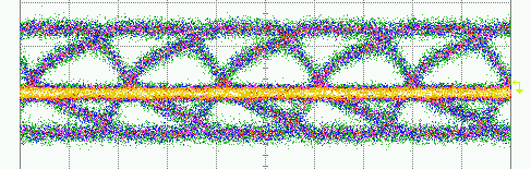
So, I have tried to use the Custom PHY, however I get some weird data at the output. Attached is the eye diagram. The line is overlapping with the eye diagram as a result of the fact that the bit clock and the signal that puts the transceiver in idle state are not locked, so they appear overlapped. However, I would have expected that that line coincides with the low level ('0'). I don't know if it matters that I terminate one of the differential outputs and use it as a single-ended to connect it to equipment...Also, could you tell me what exactly does the tx_forceelecidle do? I have read that the transceiver buffer is put in an idle state, but does that mean exactly? Is there no data transmission at all, are '0' sent or what...?
- Altera_Forum--- Quote Start --- To stop the data transmission at the serial output, you can tri-state the TX serial output by controlling the tx_forceelecidle input port if you are using the Custom PHY or tx_std_elecidle if you are using Native PHY. You may refer to the transceiver PHY IP user guide for further details by looking up these ports. --- Quote End --- I was actually using the Low Latency PHY, however maybe I can try to replace the PHY and see if it will work. Thanks :)
- Altera_Forum
Hi Vaka,
As mentioned by ah_zhi02, you can try to mux the parallel data fed into the TX parallel input. However, you will still need to switch between your data pattern and another dummy pattern. Like what you have mentioned, the transceiver will work continuously. Note that if you have the 8b10b block enabled, even if you are sending 0x00, you will still see toggling at the TX serial output due to the 10b encoded data.