programmable logic device
454 Topics
Leakage Current in MAX 10 Bank 1A (ADC Bank)
Device:10M08DCF256I7G We have connected the following voltage divider circuit to each of Bank 1A and Bank 8 of the MAX 10 device. 12 V → 10 kΩ / 3.6 kΩ voltage divider → MAX 10 input (typical voltage: 3.18 V) The measured voltages at each bank are as follows: Bank 8: 3.17 V Bank 1A: 3.06 V The voltage at Bank 1A is lower than that at Bank 8. We checked the 12 V input voltage and resistor tolerances, but found no deviations large enough to account for this difference. We also found the following statements in the datasheet: ////////// The values in the table are specified for normal device operation. The values vary during device power-up. This applies for all VCCIO settings (3.3, 3.0, 2.5, 1.8, 1.5, 1.35, and 1.2 V). 10 µA I/O leakage current limit is applicable when the internal clamping diode is off. A higher current can be the observed when the diode is on. Input channel leakage of ADC I/O pins due to hot socket is up to maximum of 1.8 mA. The input channel leakage occurs when the ADC IP core is enabled or disabled. This is applicable to all Intel MAX 10 devices with ADC IP core, which are 10M04, 10M08, 10M16, 10M25, 10M40, and 10M50 devices. The ADC I/O pins are in Bank 1A. ////////// Could you please confirm whether it is reasonable to conclude that this phenomenon is caused by leakage current specific to Bank 1A (the ADC bank)?25Views0likes3CommentsInvestigation of HIGH-Level Voltage Fluctuations on MAX 10 3.3 V LVTTL Output Signals
We are investigating the cause of fluctuations in the HIGH-level voltage of a 3.3 V LVTTL output signal from the MAX 10 FPGA. Device Part Number: 10M08DCF256I7G HIGH-Level Voltage: 2.8 V to 3.3 V 1.Verification of BANK Power Supply Stability We compared the BANK power supply voltage with the signal voltage and confirmed that the power supply voltage remains stable even when fluctuations occur in the signal voltage. 2.Relationship with the Connected Device (Under Investigation) Connection: MAX 10 → [3.3 V LVTTL, 8 mA] → DS90CR287 ・Changing the damping resistor from 22 Ω to 0 Ω did not affect the issue. Could you please advise us on the possible causes of this issue and any additional aspects we should investigate?33Views0likes3Comments
Cyclone IV drop in replacement confirmations
Dear Altera, If the BANK VCCIO is 1.8V and the same package but with different LE # FPGA is drop in replace. Where the original pin is a VCCA while different LE size same pin is a IO. With 1.8V on VCCIO and input fixed to VCCA aka 2.5V do this introduce any issue? As we can see the datasheet mentioned the DC input accept 3.6 or below. -> Table 1–4. Recommended Operating Conditions for Cyclone IV GX Devices (Part 2 of 2) So the C4 device have a protection forward diode to clamp the voltage when IO is set to input? As long as that pin is fixed to input state do this condition function properly? Thanks, BrianSolved309Views0likes13Comments
Schematics/layout for TerasIC SoCKit rev. D with Cyclone V
Greetings! I am working with an ALTERA/TerasIC SoCKit development board for Cyclone V. I've downloaded the "SoCKit CD-ROM ( rev. D Hardware )" archive from www.terasic.com.tw, but it does not contain schematics or PCB layout files. What I want to do is access ~8 GPIO pins on the board, but it does not have a GPIO header. So I can either solder to the mysterious "AD-DA HDR" connector plus some LEDs/switches, or connect to one of the 3 groups of pins on the wide HSMC (one has 20 differential pairs, the other two have 60 pins each) using a Samtek connector. To do that, I need to know how the pins on the SoCKit's PCB connectors map to the 5CSXFC6D6F31C6 IC's pads. BTW, I really appreciate the board having pads for an Altera JTAG connector pads: EthernetBlaster can be used with it! --A.123Views0likes6CommentsAgilex 3 PLL in Source Synchronous mode ?
Surprisingly, the compilation fails when we try to set a PLL in source synchronous mode in an Agilex 3, while this works as expected in Agilex 5. Compiles in "direct" mode. The pin assignment comes from the Atum A3-nano but we tried various dedicated clock inputs to no avail. The error messages are a bit puzzling too (I think there are 11 PLLs in the A3CZ135BB18AE7S ) : Error (14566): The Fitter cannot place 1 periphery component(s) due to conflicts with existing constraints (1 IOPLL(s)). Fix the errors described in the submessages, and then rerun the Fitter. The Intel FPGA Knowledge Database may also contain articles with information on how to resolve this periphery placement failure. Review the errors and then visit the Knowledge Database at https://www.intel.com/content/www/us/en/support/programmable/kdb-filter.html and search for this specific error message number. Error (175001): The Fitter cannot place 1 IOPLL, which is within IOPLL IP pll_altera_iopll_2110_hws7ggy. Info (14596): Information about the failing component(s): Info (175028): The IOPLL name(s): u_pll|iopll_0|tennm_ph2_iopll Error (16234): No legal location could be found out of 5 considered location(s). Reasons why each location could not be used are summarized below: Error (23527): No route for refclk connection from "CLOCK0_50~CLUSTER" to "u_pll|iopll_0|tennm_ph2_iopll". Promote refclk to a global clock or use a dedicated IOPLL refclk pin. (4 locations affected) Info (175029): IOPLL_X106_Y53_N346 Info (175029): IOPLL_X121_Y31_N846 Info (175029): IOPLL_X106_Y2_N346 Info (175029): IOPLL_X1_Y3_N346 Error (175006): There is no routing connectivity between the IOPLL and the IOPLL Error (175022): The IOPLL could not be placed in any location to satisfy its connectivity requirements Info (175029): 1 location affected Info (175029): IOPLL_X121_Y6_N846 Error (15307): Cannot apply project assignments to the design due to illegal or conflicting assignments. Refer to the other messages for corrective action. Error (16297): An error has occurred while trying to initialize the plan stage. Error: Quartus Prime Fitter was unsuccessful. 8 errors, 11 warnings -------------------------------------------- This is very annoying for source synchronous interfaces (like RGMII). Test case available indeed.287Views0likes14Comments
Cyclone 4 PS Configuration Timing Parameters
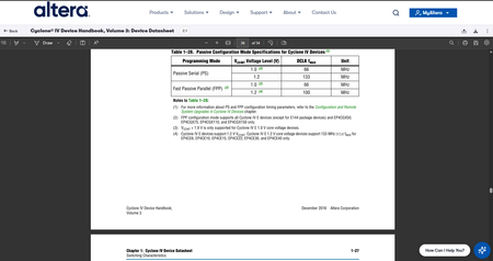
Hi, I would like to know the PS Configuration Timing Parameters for the FPGA cyclone 4 family. However, there are no indication in the datasheet: https://docs.altera.com/v/u/docs/654327/cyclone-iv-device-handbook-volume-3-device-datasheet In page 1-26 (36/54), the file sends to another file (see note 1): but that leads to a 404 error: https://www.altera.com/literature/hb/cyclone-iv/cyiv-51008.pdf Where could I find the information I require? Thank you in advance for your assistance, ChristopheSolved112Views0likes3Comments 330Views0likes6Comments
FPGA simulation and real HW behavior discrepancy
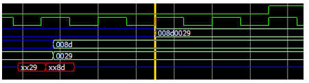
Dear Altera Quartus 18.1 sim lib could try 20.1 or newer but not sure this is due to Quartus version as it is sim lib. I am encounter an unexplainable experiment result that contradicts simulation and real HW. Background when interfacing a DQS DQ readout a IDDR with CCD sync flops are used. For these primitives, it should expected 1 + 2 and clock +ve edge should expect data push out. [A] This can simply considered as early push out but it should not act as such. With the use of "__ALTERA_STD__METASTABLE_SIM" we expected some metastable on the output. [B] Now things are more reasonable where 2 +ve clocks are expected. If we consider a full data w/o xx, things become unrecognizable. [C] The most interesting part when apply on real HW, it do produce correct data and the latencies do obeyed. altddio_in#( .intended_device_family ( "Cyclone IV E" ), .invert_input_clocks ( "ON" ), .lpm_hint ( "UNUSED" ), .lpm_type ( "altddio_in" ), .power_up_high ( "OFF" ), .width ( 8 ) )ddi_d_l( .aclr (reset), .datain (foo[7:0]), .inclock (bar[0]), .dataout_h (foobar_h[0+:8]), .dataout_l (foobar_l[0+:8]), .aset (1'b0), .inclocken (1'b1), .sclr (1'b0), .sset (1'b0) ); + altera_std_synchronizer_bundle#( .width (foobar_bw *2), .depth (2) )async_flops( .clk (clock), .reset_n (~reset), .din (foobar), .dout (foobar_ccd) );101Views0likes1Comment
Introducing the Altera Community AI Responder — Beta
Altera is introducing the AI Responder, an assistant built into the Altera Community to help provide faster, context-aware guidance for Altera product questions. It uses relevant public Altera documentation and Knowledge Database content, with coverage continuing to expand. The AI Responder may provide source references and can hand off complex or out-of-scope questions to an Altera subject-matter expert. As a beta feature, responses may contain errors or omissions, so please review the sources and verify technical guidance against official Altera documentation before implementation. If the response does not fully address your question, add more context and tag ai_responder to continue the discussion. We welcome your feedback as we improve the Community experience.32Views0likes0Comments