pcie
174 Topics
[PCIE_DESIGN_EXAMPLE][AGILEX7][QUARTUS25.3.0] - failed at elaboration process
Hello, I am trying to simulate with questa fe the pcie design example (with pipe mode for external dma controller) based on agilex7 generated with quartus pro 25.3.0 but i am facing these issues when i run this script under "pcie_ed_sim_tb/pcie_ed_sim_tb/sim/mentor" as follow : vsim -do run_msim.tcl # ** Warning: (vsim-3008) [CNNODP] - Component name (i_pclk__x16_l0) is not on a downward path. # Time: 0 fs Iteration: 0 Instance: /pcie_ed_sim_tb/dut_pcie_tb_ip/dut_pcie_tb/tile File: ../../../../support_logic/pcie_ed_sim_auto_tiles.sv Line: 34589 # ** Error: (vsim-3043) Unresolved reference to 'i_pclk__x16_l0' in ftile_s20_v0__pcie__tile_0.z1577b.z1577b_inst.i_pclk__x16_l0. # Time: 0 fs Iteration: 0 Instance: /pcie_ed_sim_tb/dut_pcie_tb_ip/dut_pcie_tb/tile File: ../../../../support_logic/pcie_ed_sim_auto_tiles.sv Line: 34589 # ** Warning: (vsim-3008) [CNNODP] - Component name (i_pclk__x4_l12) is not on a downward path. # Time: 0 fs Iteration: 0 Instance: /pcie_ed_sim_tb/dut_pcie_tb_ip/dut_pcie_tb/tile File: ../../../../support_logic/pcie_ed_sim_auto_tiles.sv Line: 34589 # ** Error: (vsim-3043) Unresolved reference to 'i_pclk__x4_l12' in ftile_s20_v0__pcie__tile_0.z1577b.z1577b_inst.i_pclk__x4_l12. # Time: 0 fs Iteration: 0 Instance: /pcie_ed_sim_tb/dut_pcie_tb_ip/dut_pcie_tb/tile File: ../../../../support_logic/pcie_ed_sim_auto_tiles.sv Line: 34589 # ** Warning: (vsim-3008) [CNNODP] - Component name (i_pclk__x4_l4) is not on a downward path. # Time: 0 fs Iteration: 0 Instance: /pcie_ed_sim_tb/dut_pcie_tb_ip/dut_pcie_tb/tile File: ../../../../support_logic/pcie_ed_sim_auto_tiles.sv Line: 34589 # ** Error: (vsim-3043) Unresolved reference to 'i_pclk__x4_l4' in ftile_s20_v0__pcie__tile_0.z1577b.z1577b_inst.i_pclk__x4_l4. # Time: 0 fs Iteration: 0 Instance: /pcie_ed_sim_tb/dut_pcie_tb_ip/dut_pcie_tb/tile File: ../../../../support_logic/pcie_ed_sim_auto_tiles.sv Line: 34589 # ** Warning: (vsim-3008) [CNNODP] - Component name (i_pclk__x8_l8) is not on a downward path. # Time: 0 fs Iteration: 0 Instance: /pcie_ed_sim_tb/dut_pcie_tb_ip/dut_pcie_tb/tile File: ../../../../support_logic/pcie_ed_sim_auto_tiles.sv Line: 34589 # ** Error: (vsim-3043) Unresolved reference to 'i_pclk__x8_l8' in ftile_s20_v0__pcie__tile_0.z1577b.z1577b_inst.i_pclk__x8_l8. # Time: 0 fs Iteration: 0 Instance: /pcie_ed_sim_tb/dut_pcie_tb_ip/dut_pcie_tb/tile File: ../../../../support_logic/pcie_ed_sim_auto_tiles.sv Line: 34589 # ** Warning: (vsim-3008) [CNNODP] - Component name (i_rxpipe0__dirfeedback) is not on a downward path. # Time: 0 fs Iteration: 0 Instance: /pcie_ed_sim_tb/dut_pcie_tb_ip/dut_pcie_tb/tile File: ../../../../support_logic/pcie_ed_sim_auto_tiles.sv Line: 34589 # ** Error: (vsim-3043) Unresolved reference to 'i_rxpipe0__dirfeedback' in ftile_s20_v0__pcie__tile_0.z1577b.z1577b_inst.i_rxpipe0__dirfeedback. # Time: 0 fs Iteration: 0 Instance: /pcie_ed_sim_tb/dut_pcie_tb_ip/dut_pcie_tb/tile File: ../../../../support_logic/pcie_ed_sim_auto_tiles.sv Line: 34589 # ** Warning: (vsim-3008) [CNNODP] - Component name (i_rxpipe0__linkevaluationfeedbackfiguremerit) is not on a downward path. # Time: 0 fs Iteration: 0 Instance: /pcie_ed_sim_tb/dut_pcie_tb_ip/dut_pcie_tb/tile File: ../../../../support_logic/pcie_ed_sim_auto_tiles.sv Line: 34589 # ** Error: (vsim-3043) Unresolved reference to 'i_rxpipe0__linkevaluationfeedbackfiguremerit' in ftile_s20_v0__pcie__tile_0.z1577b.z1577b_inst.i_rxpipe0__linkevaluationfeedbackfiguremerit. # Time: 0 fs Iteration: 0 Instance: /pcie_ed_sim_tb/dut_pcie_tb_ip/dut_pcie_tb/tile File: ../../../../support_logic/pcie_ed_sim_auto_tiles.sv Line: 34589 ..... I also have followed the Altera recommendations : Note: Due to a problem in the Quartus ® Prime Pro Edition Software version 25.3, you are required to add "-suppress 2732" to USER_DEFINED_COMPILE_OPTIONS and "-suppress 10000 " to USER_DEFINED_ELAB_OPTIONS in the run_msim.tcl simulation script manually for a successful simulation with the Questa simulator. But i am still facing these above issues. What can i do ? Regards, Frederic22Views0likes1Comment
R-TILE PIPE DIRECT MODE SIMULATION PHY STATUS ISSUE IN RESET RELEASE SEQUENCE
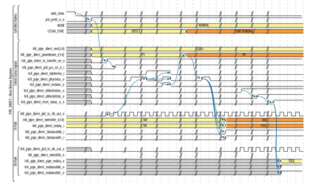
HI, I am currently working on r-tile pipe direct mode simulation in questasim. So, initially i have generated r-tile ip with configuration of pipe direct mode, 16x1. I have generated hdls using generate hdl option(enabling verilog,questasim). I have written pipe control fsm to provide control inputs to r-tile ip. Ref_clock1,ref_clock2 frequency is 100mhz. Reconfig_clock frequency is 100mhz. pipe_direct_pld_tx_clk_out_o from ip is 500mhz(validated in sim) So, i start with providing ninit_done using reset release ip. once nint_done goes low, i am providing pin_perst_n to high. then pin_perst_n_o goes high. After sometime, pipe_direct_pld_tx_clk_out_o becomes active. So, i am waiting for ln0_pipe_direct_tx_transfer_en_o to goes high. once this signal goes high, i will release ln0_pipe_direct_pld_pcs_rst_n_i to high. I am checking the phy signal to toggle. but from beginning itself it stays low, it never toggles. Along with this standard procedure, i tried 2 more possibilities i tried, After i released the ln0_pipe_direct_pld_pcs_rst_n_i to high. I provided the ln0_pipe_direct_txdetectrx_i to high. No response from phy_status. After i released the ln0_pipe_direct_pld_pcs_rst_n_i to high. I provided the ln0_pipe_direct_txdetectrx_i , rx_standby to high. still No response from phy_status I am attaching some screenshots of waveforms. Kinly look into it and help me out. I am really stuck at midway..28Views0likes2CommentsTerasic P16E-FMCP PCIE Express 3.0 compatibility issues with AMD processors
Hi I bought the Terasic P16E-FMCP to use on my Terasic Apollo S10 SOM board for PCI Express 3.0 implimentation. However after testing the included program, it did not work, so I emailed Terasic Support and they told me it was only tested on Intel CPU and it appears never tested on AMD. So they made me run a simple program called System Information Viewer from rh-software.com which tested the information sent and received from the PCI endpoint and it appears there are errors stimming back from the demo program does not natively run on AMD processors. So for the past 6 months, Terasic has been dragging there feet on this issue, telling me they will work on a solution but I must go out and purchase another computer by Intel, then run several versions of Quartus Pro, starting from 19.1, through 23.3, I must download them individually. I told them I am not doing this, I am not being paid to test out your code, I simply purchased the board direct from you for $650, and NOWHERE on the website does it publish it works only with Intel CPU. Instead they are pointing the fingers at me saying I'm delayin a resolution on this issue by not testing out there code, I told them that IS YOUR JOB! I AM NOT EMPLOYED BY TERASIC! Terasic is a partner program of Intel, they have all the means to reach out and contract a device driver writer and solve this incompatiblity issue. This is beyond my expertise. They simply won't do it. Does anyone have a solution to this problem? Why are they passing the buck at me?88Views0likes4Comments
Agilex7 M PCIe MCDMA: debug toolkit attachment
Hi, I'd need advice on how to connect Quartus PCIe Debug Toolkit to MCDMA IP in Agilex7 M. Since I'm failing to find or generate a complete example design, I'm not sure if I have to manually instantiate a JTAG Avalon master as a debug interface, or can I assume Quartus to generate the debug connection under the hood. I have read "Multi Channel DMA IP for PCI Express* Design Example User Guide" and "Multi Channel DMA IP for PCI Express* User Guide". Creating an example design of MCDMA IP configured with Debug Toolkit enabled fails on my Windows 11 machine with Quartus 25.3. Originally there was an access right problem occurring when the generation script tried to delete some temporary files in Temp under Appdata. I tried it also on workmate's PC, with the same result. After changing some user access control setting the script started failing at a later stage of processing, where it tries to read some test bench files even though I had TB files generation unchecked in parameter editor. However after the failed generation, a sample design exists. It defines all Debug Toolkit related MCDMA ports as virtual pins in .QSF. I thought this might be intentional, Quartus possibly detecting them and magically creating the missing attachment. I have this method under test, Quartus flow not yet complete. Manually using a JTAG-Avalon master component to build the debug link did pass Quartus flow, but timing between xcvr_reconfig_clk and slow_clock of PCIe MCDMA component fails as the clock relation between these two 100 MHz clocks is ~ 90 ns for some reason. I took xcvr_reconfig_clk from an internal IOPLL as the design is not an EVKIT one with suitable input clocks. Thank in advance if anyone can provide some insight.. should the example design contain more than virtual pins defined on xcvr_reconfig*, dummy_user_avmm_rst, p0_dtk_hip_reconfig_clk ? (Documented port p0_hip_reconfig does not seem to appear in my MCDMA instance.) BR Ju-TiSolved90Views0likes3Comments
PCIe stuck at reset Agilex5
Hi Altera Team, I'm trying to get PCIe connection working on our custom board. We had some problems with our design. Reset pin (CF128) is connected to CF121 on board (we forgot to connect it). At the start i set CF121 to '1', to get PCIe out of reset. When fpga boots, all clocks should be up and stable. Based on "Link Training Debugging Flow" my IP core is in reset and i should check pin_perst_n. Pin is set to '1', but IP is still in reset? What could be the couse? Is there a chance for this behaviour if core can't detect root? Do i need IO_Pll to lock for core to get out of reset? I use example design for PCIe, with different pinout. Device: A5ED065BB32AE6S - Common clock architecture49Views0likes1Comment
Agilex 7 R-Tile PCIe Gen5: Avalon-ST DMA MWr TLP accepted by HIP but never received by Root Port
I am debugging a design using the Intel mSGDMA Read Master IP connected to the Intel Agilex 7 R-Tile PCIe Gen5 Hard IP through the Avalon-ST TX interface.The design uses the Intel mSGDMA Read Master to read data from memory. The Avalon-MM read data is then packetized into PCIe Memory Write (MWr) TLPs and transmitted through the R-Tile PCIe HIP. The transmit path is: Intel mSGDMA Read Master → dma_mwr_txc_gen → txc_mux_2to1 → pcie_bam_avst_intf → pcie_pio → Agilex 7 R-Tile PCIe HIP The endpoint enumerates correctly, the PCIe link trains successfully to Gen5 x16, configuration space accesses work correctly, BAR accesses work correctly, and normal MMIO/PIO operations function as expected. The only issue occurs when transmitting DMA-generated Memory Write TLPs. We have spent considerable time verifying the transmit path using both simulation and Signal Tap, and everything appears to be correct up to the HIP interface. Specifically, we have verified the following: The Avalon-ST TX interface follows the R-Tile User Guide. SOP/EOP placement is correct. Segment valid signals are correct. Header valid and payload valid are correct. ready remains asserted throughout the transfer. No Avalon-ST protocol violations are observed. The ACC signal gets asserted after the TLP is sent to the HIP The generated Memory Write header decodes correctly (128-byte MWr, correct addresses, requester ID, and length field). Payload contents are correct. Address increments correctly between successive packets. Signal Tap shows the expected TLP immediately before entering the HIP. The HIP accepts the packet (valid and ready handshake completes). No HIP or protocol error indications are observed. However, the Root Port never appears to receive the Memory Write TLP. The expected data never becomes visible to the host software, even though the packet appears to have been accepted by the HIP. After several DMA attempts, the Root Port—or sometimes the entire server—eventually becomes unresponsive and requires a reboot. We do not observe any AER messages, completion timeout messages, or other PCIe errors reported by the operating system. We also investigated timing closure to rule out timing-related corruption. At this point, we are trying to determine whether there is something beyond the Avalon-ST interface that could cause the HIP to silently discard or otherwise fail to transmit a posted Memory Write TLP. Has anyone encountered a similar issue on the Agilex R-Tile PCIe HIP where: the Avalon-ST interface appears completely correct, the HIP accepts the packet (ready/valid handshake completes), no protocol or PCIe errors are reported, but the Root Port never receives the posted Memory Write? Are there any additional HIP status registers, debug signals, credit counters, packet validation checks, alignment requirements, or other R-Tile-specific conditions that should be examined? Are there any known situations where a posted Memory Write can be silently drop after being accepted on the Avalon-ST interface? Any suggestions on additional debug points or known R-Tile HIP behaviors would be greatly appreciated. Thank you. Reza166Views0likes1Comment
Cyclone IV GX PCIe Hard IP behaves differently on Intel Core I7 vs Xeon root complexes
Hello, I am working with a Cyclone IV GX (EP4CGX22) using the Altera PCIe Hard IP configured as PCIe Gen1 x1 with an Avalon-MM interface. The same FPGA image shows different behavior depending on the host platform. Platforms Tested Working Platform Intel Core i7-13700 Windows 11 Platforms Where the Issue Is Observed Supermicro X10SRA + Xeon E5-1620 v3 Supermicro X12SPL-F + Xeon Silver 4309Y PCIe Configuration The FPGA endpoint is configured as PCIe Gen1 x1 The Xeon platforms provide newer PCIe root complexes: Xeon E5-1620 v3 -> PCIe Gen3/4 capable slot Xeon Silver 4309Y -> PCIe Gen3/4 capable slots However, the link correctly negotiates down to: Link Width : x1 Link Speed : Gen1 (2.5 GT/s) which matches the FPGA endpoint capability. Common Observations On all platforms: PCIe enumeration succeeds Vendor ID and Device ID are detected correctly BAR resources are assigned correctly The device driver loads successfully The PCIe link is established successfully TLP as data input getting unexpected value Observed Difference Although the PCIe link is established correctly on all systems, the FPGA observes different transaction behavior on the Xeon platforms compared to the Intel Core i7 platform. The same FPGA image and software stack operate as expected on the Intel Core i7-13700 system, while different behavior is observed on both Xeon-based systems. Questions Are repeated accesses to BAR-space offsets after boot expected from BIOS/UEFI, Windows PCI bus enumeration, or other background PCIe activity? Has anyone observed different behavior between Intel Core desktop root complexes and Xeon/server root complexes when using the Cyclone IV GX PCIe Hard IP? Are there known interoperability issues between older Cyclone IV GX PCIe endpoints and modern Gen3/Gen4 server root complexes, even when the link successfully negotiates to Gen1 x1? Is there a recommended way to distinguish firmware/OS-generated PCIe accesses from accesses generated by the application or function driver? Any feedback or similar experience would be greatly appreciated. Thank you.124Views0likes6Comments
Altera Agilex PCIe core
Hi Altera Team, We have developed a user reset controller based on the "Cold Reset Entry and Exit Sequence" described in the "GTS AXI Streaming IP for PCI Express User Guide for Agilex® 5 and Agilex® 3 FPGAs and SoCs". Currently, our implementation is stalled at Step 2 of the reset sequence. Our user reset logic is waiting for the PCIe IP to assert the p<n>_initiate_warmrst_req signal; however, this signal is never asserted during simulation. Our current PCIe configuration is as follows: * PCIe x 4lanes * AXI Streaming interface: 128-bit * PLD clock: 200 MHz * Reference clock: 100 MHz * System PLL configured as required Could you please advise on the possible reasons why p<n>_initiate_warmrst_req may not be asserting? Additionally, are there any configuration settings or reset timing requirements that must be satisfied before the PCIe IP generates this signal?89Views0likes5CommentsDDR2 license Question
The customer obtained the DDR2 license through the Altera website. Does this IP license have any time limitation or other usage restrictions? When generating the project for the EP4CE75U19I7N device, Quartus only generates project.sof and does not generate project_time_limited.sof.68Views0likes4Comments
Can an Application Ignore PCIe flow Control Credits?
I'm using a Cyclone V GT with PCIe core using Gen 1 Avalon-ST 64-bit endpoint interface. Occasionally packet sending would stall and I had thought it was because I was ignoring the flow control credits. But after properly handling tx_st_ready going low, the problem seems to have gone away. So the question is can I ignore the flow control signals as long as I throttle the sending when tx_st_ready goes low? In the flow control section of the UG-011110 dated 2020.06.02, it says That is not important for our application. But then after spending several paragraphs explaining how the PCIe Hard IP tracks and checks credits, it make says: Can I assume that is only in the case described in the yellow highlight? Also, in the flow control update loop description, is says: Is that where the Hard IP is lowering tx_st_ready so the App is indirectly handling credits? If so, one odd thing is that sometimes tx_st_ready does not go low until toward the end of a packet write (ie closer to the EOP and the SOP). I would think it would do the credit check as soon as it had the TLP headers which contain the type, number of dwords etc. Just a suggestion, but for Apps that did want to optimize throughput, it would have been helpful to just expose the credit limits to the App instead of making it independently keep track of them. The credit system is a bit confusing.Solved115Views0likes5Comments