Forum Discussion

 Contributor
How to handle tx_st_ready for Cyclone V PCIe
I'm using a Cyclone V GT with PCIe core using Gen 1 Avalon-ST 64-bit endpoint interface. Everything works pretty well including sending and receiving data, DMA transfers etc. But so far I've ignored the situation where tx_st_ready is deasserted during a packet transmission. Time to deal with it, but the docs are a bit confusing.
For example, the following implies I have some sort of control over the readyLatency, but I see nothing in the core generator to set that. How to I know what the readyLatency is?
And what to they mean the "typical case"?
In the above, are they saying I should register them? I see nothing in the core generator to say if they should be registered or not.
They give a timing diagram below which is a bit confusing.
Hi corestar
I noticed the screenshot in your post appears to be from the older and obsolete user guide (Cyclone® V Hard IP for PCI Express* User Guide). While this document may still be accessible through internet searches, it has been removed from the official Altera documentation site, see this KDB: https://community.altera.com/kb/knowledge-base/why-is-the-cyclone%C2%AE-v-hard-ip-for-pci-express-user-guide-page-not-found/347580
To access the latest documentation, please use the following resources:- PCIe Support Center: https://www.altera.com/design/fpga-ip/pcie-support
For PCIe documentation, the best starting point is the PCIe Support Center. This page consolidates PCIe user guides across all supported device families. - Altera Documentation & Resources Center: https://docs.altera.com/
Since you are using the Avalon-ST interface, please refer to the Cyclone® V Avalon® Streaming (Avalon-ST) Interface for PCIe Solutions User Guide*. You can find the user guide link in the provided KDB, PCIe Support Center, and Altera Documentation & Resources Center.
I also noticed that the timing diagram shown in your screenshot (Figure 7-21) has been corrected in the latest user guide revision. The updated diagram provides a clearer description of the signal behavior.
Below the is the corrected timing diagram:
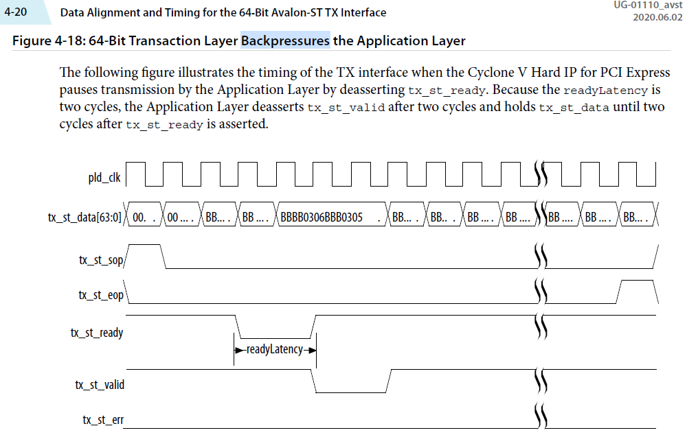
To answer your question on readyLatency:- readyLatency is not a user-selectable IP parameter in the Cyclone V PCIe IP Parameter Editor. Instead, it describes the effective handshake timing between the PCIe core and the application logic. The PCIe Hard IP drives tx_st_ready, while the application logic drives tx_st_valid and tx_st_data.
- The user guide states that when tx_st_ready, tx_st_valid, and tx_st_data are registered in the typical implementation style, Altera recommends a readyLatency of 2 cycles to facilitate timing closure; however, a 1-cycle response is also possible.
- In practice, this means:
- 2-cycle readyLatency is the recommended and easier case for timing closure
- 1-cycle readyLatency can reduce latency, but it requires a tighter ready-to-valid/data path in the user RTL and is therefore harder to meet timing.
Additionally, the Avalon-ST specification (user guide link: https://docs.altera.com/r/docs/683091/22.3/avalon-interface-specifications/synchronous-interface?tocId=LUasgm1svG8VSQd1UQY7Aw) states that source outputs toward the sink, including data, must be registered on the rising edge of the clock, which is why the registered 2-cycle implementation is considered the typical case.
I hope this answers your questions. Please let me know if any clarification is needed.
Thanks.
Best Regards,
Ven Ting- PCIe Support Center: https://www.altera.com/design/fpga-ip/pcie-support
7 Replies
 VenT_Altera
Frequent Contributor
Hi corestar
Thanks for reaching out to us.
Please allow me sometime to investigate your issue, I will get back to you with an update shortly.
Thanks.
Best Regards,
Ven Ting corestar
Hello VenT_Altera
Thanks for the update. Maybe a better way to phrase my question is are the signals in the timing diagrams (ie tx_st_ready, tx_st_valid etc ) the ones directly coming out of the core or ones externally registered by the user? Again, the way it is worded makes it sound like the user has some control over the readyLatency, but nothing in the core generator allows me to select that.
I've gone ahead and implemented it assuming readyLatency = 2 and the signals are from the core and it seems to work. But it would be nice to know for sure.
Thanks,
Dave- VenT_Altera
Hi corestar
I noticed the screenshot in your post appears to be from the older and obsolete user guide (Cyclone® V Hard IP for PCI Express* User Guide). While this document may still be accessible through internet searches, it has been removed from the official Altera documentation site, see this KDB: https://community.altera.com/kb/knowledge-base/why-is-the-cyclone%C2%AE-v-hard-ip-for-pci-express-user-guide-page-not-found/347580
To access the latest documentation, please use the following resources:- PCIe Support Center: https://www.altera.com/design/fpga-ip/pcie-support
For PCIe documentation, the best starting point is the PCIe Support Center. This page consolidates PCIe user guides across all supported device families. - Altera Documentation & Resources Center: https://docs.altera.com/
Since you are using the Avalon-ST interface, please refer to the Cyclone® V Avalon® Streaming (Avalon-ST) Interface for PCIe Solutions User Guide*. You can find the user guide link in the provided KDB, PCIe Support Center, and Altera Documentation & Resources Center.
I also noticed that the timing diagram shown in your screenshot (Figure 7-21) has been corrected in the latest user guide revision. The updated diagram provides a clearer description of the signal behavior.
Below the is the corrected timing diagram:
To answer your question on readyLatency:- readyLatency is not a user-selectable IP parameter in the Cyclone V PCIe IP Parameter Editor. Instead, it describes the effective handshake timing between the PCIe core and the application logic. The PCIe Hard IP drives tx_st_ready, while the application logic drives tx_st_valid and tx_st_data.
- The user guide states that when tx_st_ready, tx_st_valid, and tx_st_data are registered in the typical implementation style, Altera recommends a readyLatency of 2 cycles to facilitate timing closure; however, a 1-cycle response is also possible.
- In practice, this means:
- 2-cycle readyLatency is the recommended and easier case for timing closure
- 1-cycle readyLatency can reduce latency, but it requires a tighter ready-to-valid/data path in the user RTL and is therefore harder to meet timing.
Additionally, the Avalon-ST specification (user guide link: https://docs.altera.com/r/docs/683091/22.3/avalon-interface-specifications/synchronous-interface?tocId=LUasgm1svG8VSQd1UQY7Aw) states that source outputs toward the sink, including data, must be registered on the rising edge of the clock, which is why the registered 2-cycle implementation is considered the typical case.
I hope this answers your questions. Please let me know if any clarification is needed.
Thanks.
Best Regards,
Ven Ting - PCIe Support Center: https://www.altera.com/design/fpga-ip/pcie-support
- VenT_Altera
Hi corestar,
As there are no further inquiries, I will transition this thread to community support. If you have a new question, feel free to open a new thread to get support from Altera experts.
Have a great day!
Thanks.
Best Regards,
Ven
- corestar

