fpga devkit
894 Topics
Installer Package for DK-DEV-10AX115S-B
The Obsolete Arria® 10 GX FPGA Development Kit | Altera revision -A came with an Installer package: The Arria® 10 GX FPGA Development Kit | Altera revision -B is missing this: Can you please provide similar resources? Best regards, Nikolay12Views0likes1Comment
Proper PERST# connection for FMC on Agilex5 Modular Development Kit
I am using an Agilex5 Modular Development Kit to implement a design that has two PCIe endpoints. Each endpoint would run at the same x4 configuration (start with Gen3 and maybe move to Gen4). The first endpoint is easy as the board supports it natively. For the second endpoint I am planning to use the Terrasic P16E-FMCP board and use a separate adapter to limit the width to x4. I went through the schematic several times and I am fairly confident that FMC PCIe lanes 0-3 (plus the reference clock) would connect to the transceiver bank 1B on the Agilex5 device. So the high speed signals look to be OK. My issue is with how to achieve a proper PERST connection. The FMC board connects the PERST# signal to the FMC RES0 pin which is not connected on the Agilex board. This means I have to make a manual connection to the appropriate pins on the FPGA device. Assuming that my bank 1B analysis is correct then the possible PERST# pin connections are: CF132 net A5E_HVIO_5A_6 IO_D61 pin on the primary board-to-board connector Carrier board: net MIPI_XHS0_1V8 which is floating if there is nothing plugged to the MIPI connector Manual PERST connection: Level shift the PERST signal down to 1.8V and then solder it to the MIPI_XHS0_1V8 net. BU109 net A5E_HVIO_5B_6 IO_A56 pin on the primary board-to-board connector Carrier board: BMC_UART_RX0_I2C_SCL_3V3 which is connected to the MAX10 device Manual PERST connection not possible Before I do the board modification, I would like to confirm my analysis is correct (maybe 1B is not the correct bank) and that I am not missing some other, easier, connection. Thank you very much in advance. Any help is greatly appreciatedSolved438Views0likes7CommentsHelp needed to start PAM4 loopback test on Stratix 10TX-SI Kit
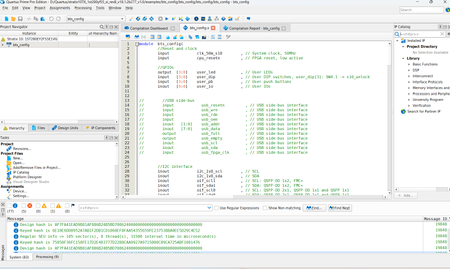
Hi everyone, I am working with the Stratix 10 TX Transceiver Signal Integrity Development Kit and I am trying to run the PAM4 loopback test. I have followed the documentation and found both qts_pam4_com and bts_pam4.sof. I’m currently in Quartus with the bts_config project open, but I’m stuck on how to proceed to the BTS main page → PAM4 tab. Could someone please clarify the correct sequence for: bts_pam4.sof → FPGA configuration → launch qts_pam4_com/BTS → PAM4 tab → start QSFP-DD/2.4-mm loopback test? Do I need to compile bts_config, or can I directly use bts_pam4.sof? Any guidance would be greatly appreciated. Thanks! Kind,29Views0likes2CommentsBoard Test System Download Package – Stratix 10 TX Signal Integrity Development Kit
Hello, I am currently working with the Stratix 10 TX Signal Integrity Development Kit on a Windows PC and would like to use the Board Test System (BTS) to verify the functionality of the board. According to the Stratix 10 TX Transceiver Signal Integrity Development Kit User Guide, the BTS application should be included in the development kit package under: <package_dir>\examples\board_test_system\BoardTestSystem.exe However, I have not been able to locate the appropriate BTS package or download containing the BoardTestSystem.exe application. Could someone from Altera please provide the current download link or the appropriate installer/ZIP package containing the BTS application and its associated test designs (.sof files)? I would also appreciate confirmation of the recommended Quartus Prime version and any required dependencies for running the BTS on Windows. Board: Stratix 10 TX Signal Integrity Development Kit Development Kit: DKSI1STXEA Host OS: Windows Thank you for your assistance.543Views0likes8CommentsWorkaround for TCK frq. limitations on USB-Blaster I/II/III & Clones (fixing "JTAG chain broken")
Workaround for TCK frequency limitations on USB-Blaster I/II/III and clones (fixing "JTAG chain broken") Hi everyone, I'd like to share a practical workaround for a problem many of us run into when programming Altera FPGAs through test fixtures, level shifters or long ribbon cables. **The problem** In these setups, "JTAG chain broken" or "Unable to scan device chain" errors are common. They are usually caused by signal reflections and poor termination on custom boards and long extensions. Lowering the TCK frequency is the standard remedy, but the options are limited: - USB-Blaster I (and most low-cost clones) runs at a fixed TCK of about 6 MHz. Quartus offers no way to change it. - USB-Blaster II can be set to 6/16/24 MHz via `jtagconfig --setparam <cable> JtagClock <freq>`, but nothing below 6 MHz. In practice this setting is also unreliable: it is not persistent and can fall back to the 24 MHz default (see Altera KB: "Why does the TCK frequency setting of the USB-Blaster II download cable revert to the default value of 24 MHz after being changed?"). In our experience it is a constant source of trouble, especially in production where it has to be set again and again. For really marginal lines, 6 MHz is often still too fast. **The workaround** Disclosure: I'm the developer of the tool described below, so please take this as information from the vendor. Quintus Programmer (by Dution) drives the JTAG lines of the USB-Blaster in bit-bang mode instead of using the adapter's fixed shift clock. This lets you choose the TCK frequency freely, e.g. down to 100 kHz, with the same USB-Blaster I/II/III or clones you already have. With a lower TCK, programming and verification become stable again on long or poorly terminated lines without any hardware changes. The standard USB-Blaster driver stays in place, and Quintus only replaces the programming step. **Before reaching for software, check the hardware basics** The recommendations from the Altera Knowledge Base still apply and often fix the problem on their own: - TCK pull-down 1 kΩ to GND, TMS/TDI pull-up 10 kΩ to VCCIO - a small capacitor (10–22 pF) at TCK near the FPGA against ringing edges - a TCK buffer on long or noisy lines If the layout can't be changed, a lower TCK is a practical way out. More info: search for "Quintus Programmer Dution". Happy to answer technical questions here.171Views0likes2CommentsRev B Arria 10 development kit
Rev A / Power Solution 1 DK-DEV-10AX115S-A Product page: https://www.altera.com/products/devkit/po-3017/arria-10-gx-fpga-development-kit Rev B / Power Solution 2 DK-DEV-10AX115S-B Product page: https://www.altera.com/products/devkit/po-3320/arria-10-gx-fpga-development-kit We are looking early into Rev B version of Arria 10 dev.kit. I can't found any BOM yet, and I would like to know if flash components were changed? At least EPQCL flash is inconveniently under heat sink and fans. I would like not to replace thermal compound.263Views0likes2Comments
Introducing the Altera Community AI Responder — Beta
Altera is introducing the AI Responder, an assistant built into the Altera Community to help provide faster, context-aware guidance for Altera product questions. It uses relevant public Altera documentation and Knowledge Database content, with coverage continuing to expand. The AI Responder may provide source references and can hand off complex or out-of-scope questions to an Altera subject-matter expert. As a beta feature, responses may contain errors or omissions, so please review the sources and verify technical guidance against official Altera documentation before implementation. If the response does not fully address your question, add more context and tag ai_responder to continue the discussion. We welcome your feedback as we improve the Community experience.19Views0likes0Comments
Design of MAX V CPLD 5M2210 System Controller in Arria 10 SoC board
Hi Altera, Could you help to share the MAX V CPLD 5M2210 System Controller with me? We're in AI research work with Arria 10 SoC board and need the source code of system maxV but is not included in the installer package, arria10_10as066n3f40_soc_v15.1.2.zip. Thank you!430Views0likes7CommentsWhy 390.625MHz clock to F-Tile Reference fequency
Hi, This question is regarding the Agilex 7 M-Series FPGA Development Kit. In the evaluation board schematics, the Si5518 provides a 390.625 MHz clock that is connected to two F-Tile reference clock inputs. From the F-Tile Ethernet Hard IP User Guide, I understand that standard Ethernet designs typically use 156.25 MHz as the PMA reference clock, while the 390.625 MHz clock appears internally as the clk_txmac/clk_rxmac clock. My questions are: 1. Which F-Tile configuration or interface is intended to use the external 390.625 MHz reference clock on the development board? 2. Is this reference intended for the Ethernet Hard IP, PMA Direct mode, SyncE, or some other transceiver application? 3. Are there any official reference designs that use this 390.625 MHz reference clock? I would appreciate it if you could clarify the intended use of this clock on the Agilex M Development Kit. Regards,618Views0likes6CommentsBoard Test System–Stratix 10TX Development Kit
Hi everyone, I’m working with the Stratix 10 TX Signal Integrity Development Kit (DKSI1STXEA) on a Windows PC. I have followed the installation steps provided in the documentation and installed the development kit software/package as instructed. However, after completing the installation, I still cannot find the Board Test System (BTS) files. According to the user guide, I expected to find something similar to: <package_dir>\examples\board_test_system\BoardTestSystem.exe I have not been able to locate the associated .sof test designs either. Has anyone successfully installed and used the BTS for this development kit? Could someone please clarify which package needs to be installed to get the BTS files, or where these files are located in the current version of the development kit software? Board: Stratix 10 TX Signal Integrity Development Kit Kit: DKSI1STXEA Host OS: Windows I have already followed the documented installation procedure, but the BTS files still appear to be missing. Any help would be appreciated. Thank you!Solved180Views0likes6Comments