fpga devkit
894 Topics
Arria 10 GX Remote Update Circuitry
Hello, We are using an 10AX066 FPGA connected to an MT25QU01 flash. It's connected through Active Serial. We are looking to use a system setup that will allow us to boot into a user image, before falling back to a factory image if it fails to configure 3 times, we do not need a watchdog, or the AnF bits. Is the default behaviour of the Arria 10 device to provide the features provided in this flow chat (https://www.intel.com/content/www/us/en/docs/programmable/683461/current/configuration-sequence-in-the-remote.html)? Is the Remote Update IP core necessary for any functions that we want?1.1KViews2likes2Comments
in MAX 10 Dev kit
Hi Altera Community, I am encountering a JTAG Server Error Code 35 when attempting to program my MAX 10 Development Kit using the USB-Blaster. Below are the details of my setup and the issue: Board: MAX 10 Development Kit Programmer Cable: USB-Blaster Problem Description: When opening the Quartus Programmer and clicking Start (or running Auto Detect), the process fails with the following log: Error (209053): Unexpected error in JTAG server -- error code 35 Error (209040): Can't access JTAG chain189Views1like6Comments
Cyclone V GT Dev Kit - new units fail to boot from FPP
We have been using this development kit internally for many years, and on our last order 2 out of 3 units fail to boot using the Fast Passive Parallel (FPP) configuration scheme through the MAX V. We normally use our own custom MAX V bitstream, but the issue is present even with the factory MAX V image and the factory FPGA image/flash content. The MAX V appears to try loading the image (LED D6 flashing or statically lit, depending on the MAX V firmware version) for about 6 seconds before giving up and signaling an error (LED D5). On reception, one of the two faulty boards seemed to work, it was just taking a bit longer to boot than usual (presumably it took a few retries). It then got progressively worse: the boot started failing intermittently, and now it is almost impossible to get it to boot through FPP. The boards can still boot through Active Serial (AS), and the FPGA can properly read and write the main flash, so the issue seems to affect only the MAX V flash access / FPGA configuration. Following this thread, which reports the same issue: Cyclone VGT Dev Kit boards - some new boards failing to boot from NOR Flash | Altera Community - 353984 we tried reducing the MAX V utilization to improve timing. With this change one of the boards managed to boot a few times, but very rarely and not reliably. The affected boards are all rev. B and have serials: - 5CPCIE00100214 - 5CPCIE00100263 While debugging, I also noticed that the timing constraints do not follow the Parallel Flash Loader IP User Guide. For example, fpga_dclk should be a generated clock and used as the reference for the other constraints, and the set_output_delay on fpga_data does not respect the tDSU from the Cyclone V datasheet. That said, correcting these constraints did not improve the boot behavior. We are now stuck with two boards that can only boot from AS, which is a concern for future orders. Between this and the flash revision change to rev. B (where the PCB is actually labelled rev. A and the example designs are mixed and not clearly labelled), these boards are becoming difficult to work with. Since there is at least one other thread reporting the same behavior it looks less like an isolated fault and more like a recurring issue on recent production. Could someone from Altera confirm whether this is being tracked, and what the recommended action is for affected boards?Solved413Views1like13Comments
Cyclone VGT Dev Kit boards - some new boards failing to boot from NOR Flash
We've been using these boards for years, having certified them for use in one of our products. In the last few months we have now received 5 of these boards and they fail to configure from NOR flash. These are all the new Rev B CVGT Dev Kit edition. Not all of the new RevB fail, but the fail rate is high, getting close to 50%. Yes, we know they changed to a Micron NOR flash for Rev B and rerouted some data lines, we are using the new RevB MAX5 files and have updated the Cyclone V NOR flash pins to match as well. I made some diagnostic changes to the MAX5 boot source (I set the PGM leds to count retries) and discovered that on the bad boards, the boot process goes through multiple configuration retries and eventually the watchdog timer fires, turns on the ERR (D5) red LED and stops. With the factory image they come with, there are also dozens of retries, then sometimes the boards fail, sometimes they boot up. With the slow speed that the NOR flash configuration runs at, there is no reason that it should ever fail and retry, and indeed on good boards they configure the first time every time with no retries. The first four we were able to send back to Altera (Via digikey where we bought them). We just got another bad one yesterday, this one from Mouser. Has anyone else seen this issue, and/or heard from Altera about this? Board link: https://docs.altera.com/r/docs/792833/current/cyclone-v-gt-fpga-development-kit-user-guide/kit-features682Views1like25CommentsDifferential Signal Transmitter on Agilex 5 FPGA Modular Dev Kit
We will use the SOM Module of the Agilex 5 FPGA E-Series 065B Modular Development Kit (MK-A5E065BB32AES1) for a new project with our own designed carrier board. For this design we need multiple differential transmit and receive signals from I/O Bank 2A_B and 2A_T (→ 1.2V bank supply). We started with a basic design to evaluate usable I/O Standards. We have seen that we can use differential receiver with the 1.2V bank supply but it is not possible to use "True Differential Signaling" on transmit pins with 1.2V bank supply. For our purpose it is necessary to generate differential transmit signals correctly working with LVDS inputs on the receiver site. Is there an alternative differential signal output generating a correct LVDS signal for a LVDS receiver working with the 1.2V bank supply (e.g. POD12 with special termination)? What happens when setting differential transmit and receive pins to "1.3V True Differential Signaling" to get Quartus running without an error but physically using only 1.2V bank supply? Will this only decrease signal swing on transmit pins or is this not working? Or could this damage the FPGA transmit and receive pins of the FPGA? The SOM schematic does not show any possibility to disconnect the I/O Banks 2A_B and 2A_T from onboard 1.2V supply to use an alternative external 1.3V supply. Is there the a possibility to supply these banks externally by 1.3V? Which other alternatives do we have to get differential signaling output working?125Views1like2CommentsIC FPGA - EP4CE40F23C8N -Urgent
IC FPGA - EP4CE40F23C8N has a maximum number of single-ended digital inputs/ outputs of greater than 700 where in this context, the maximum number of digital inputs/outputs is also referred to as the maximum user inputs/ outputs or maximum available inputs/outputs, whether the integrated circuit is packaged or bare die.998Views1like6Comments
MAXII CPLD VGA CONTROLLER QUESTIONS
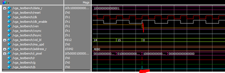
Hi there! Im doing some experiment with vga under epm570t100 for 640x480 vga controller, apparently all is quite functional per results on vga screen, however i would like any comments from your expert experience... :D. Design and simulation files attached for your reference or use. My first approach is interfacing controller with 16kx32 sram and shift each 16 bits in memory as individual pixels (black or white). 1-When interface either 16/8bit data bus i find horizontal frame barely can fit the bits(pixels), on my design, last shifted pixel at the rising edge of 25MHz clock_enable signal is just at the end of horixontal line, it is on the falling edge of the video active region... almost a glitch Per screen results when playing with first/last pixel with external switch on data bus, it appears to eat those pixels well... (3 pixels on 1920 screen resolution equivalent to 1 pixel on 640): Is this behavior to be expected?, maybe some designs extend a little the horizontal active region to fit pixels? 2-I find 2 port srams quite attractive for this application, since can write and read independently, u can see here an example of 16bits x32k one. The question is... if two cheaper one port sram is to be used, have u any experience how to manage ping-pong buffering between 2 single port stams like this one? Ie: using vsync or video enable signal to command a switch between 2 rams, one being filled the other being read.... Have u any experience on this one? Thanks in advance! Some extra photos for fun :D: All 16bits "on" 3/4 bits off all off alternated BoardSolved1.4KViews1like8Comments