New Contributor
Cyclone IV E(EP4CE30) FPGA JTAG and USB-Blaster
Hi Team,
I am working with a Cyclone IV E FPGA(EP4CE30), where all my banks (Bank 1–8) have VCCIO = 3.3V. The FPGA core voltage is 1.2V, and the PLL supply is 2.5V. I am configuring the FPGA in Passive Serial (PS) mode.
My current doubt is regarding the pull-up voltage for JTAG and USB Blaster:
Should the pull-up resistors be tied to 2.5V or 3.3V? What should be the pullup voltage for MSEL Pin..?
As per the Hardware Design Guidelines, my understanding is that the pull-up supply should match the VCCIO of the respective bank. Please confirm if this is correct.
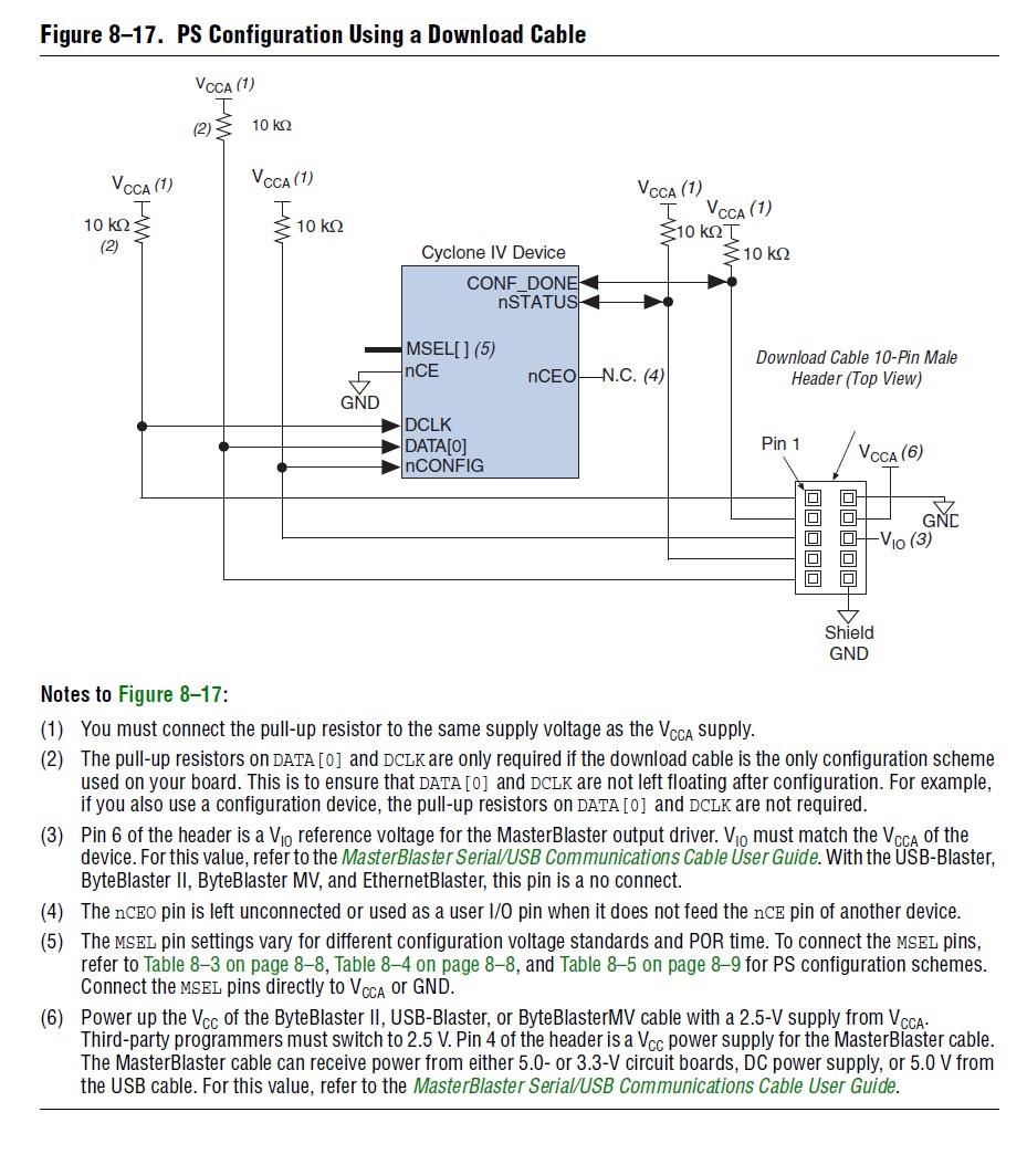
For your review, I have attached a snippet of the Configuration Pin Schematic. Kindly check and let me know if anything looks incorrect.
Additionally, for the 10-pin male header, what should be the voltage level for Pin 4 and Pin 6?
Please respond at the earliest. If you need any clarification, feel free to ask.
Thank you!
Hi,
Please connect to 2.5V VCCA even though the VCCIO of the banks where the configuration pins reside is 3.3V.
For more information, you can refer to this Knowledge Base article:
Regards,
Aqid