other ips
160 Topics
Introducing the Altera Community AI Responder — Beta
Altera is introducing the AI Responder, an assistant built into the Altera Community to help provide faster, context-aware guidance for Altera product questions. It uses relevant public Altera documentation and Knowledge Database content, with coverage continuing to expand. The AI Responder may provide source references and can hand off complex or out-of-scope questions to an Altera subject-matter expert. As a beta feature, responses may contain errors or omissions, so please review the sources and verify technical guidance against official Altera documentation before implementation. If the response does not fully address your question, add more context and tag ai_responder to continue the discussion. We welcome your feedback as we improve the Community experience.22Views0likes0Comments
MT25QL128 Not Available in ALTASMI_PARALLEL Configuration Device List
Hi everyone, I'm working on a design with Cyclone FPGA(s) in a master/slave (active/passive) configuration, using a Micron MT25QL128 flash device for FPGA configuration storage. While trying to instantiate the ALTASMI_PARALLEL IP, I noticed that the configuration device list only contains devices such as: EPCS16/64/128 EPCQ16/32/64/128/256/512 I cannot find MT25QL128 in the list. I have the following questions: What is the recommended configuration device selection in ALTASMI_PARALLEL when using a Micron MT25QL128? Is selecting EPCQ128 the correct approach since both devices are 128 Mbit? Are there any known compatibility issues between ALTASMI_PARALLEL and MT25QL128 regarding Read ID, status register access, sector erase, or page programming? When converting a SOF to a JIC file in Quartus, i can see in that list as configuration device for an MT25QL128 flash. For reference: FPGA family: Cyclone IV E Flash device: Micron MT25QL128 Configuration method: Active Serial Application: Master/Slave FPGA system with configuration stored in external flash Any guidance or experience with this setup would be greatly appreciated. Thanks!278Views0likes8Comments
Stratix 10 fPLL is cascade source mode doesn't lock
Hello everyone. I use fPLL cascading with Stratix 10 FPGA: fPLL in cascade source mode is connected to fPLL in transceiver mode. In my design reference clock for fPLL in cascade source mode is not stable after power-up and I apply user recalibration to it. But after user recalibration when reference clock is stable, fPLL doesn't set lock signal. After some investigation of the issue, I found that my design works fine with Quartus Pro 21.2 but doesn't work with newer versions like Quartus Pro 23.4/25.1/26.1. Is there any known issue about fPLL is cascade source mode? Any suggestions about how to overcome this issue are welcomed.844Views0likes19Comments
LTPI IP - any plan to support OCP LTPI Revision 1.2? (MAX 10)
Hi, We are planning to purchase the Altera LTPI IP, targeting MAX 10 (Quartus Prime Standard Edition). The LTPI IP User Guide states the IP is compliant with OCP DC-SCM 2.1 LTPI revision 1.1, version 1.1 specifications. Meanwhile the OCP LTPI reference implementation has moved to Revision 1.2 (release 1.20, 12 Dec 2025), which adds extended CRC/error handling with a new Frame Lost error, renames LTPI Version to LTPI Revision (CSR packages regenerated), and changes the Link Speed timeout and Link Lost conditions. Is there a plan to update the LTPI IP to Revision 1.2? Thanks.165Views0likes5CommentsAXI4-Lite Firewall IP core - Altera support request
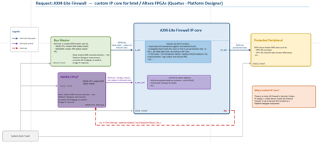
Greetings Altera, Just FYI, I writing in the community forum, in addition to a sent an inquiry yesterday, through the website contacts form - https://www.altera.com/contact - in attempt to get into contact and start a conversation going with some of your FAEs regarding a problem our company and team is facing: Currently in one of our FPGA Designs utilizing Altera FPGAs (CycloneV SoC ARM (5CSEBA5)), there is a requirement to monitor and control data streams/transfers between AXI4 master and slave devices. We have to ensure those are occurring in the allowed (configurable) address ranges, and if not, such data transfer is canceled – both downstream and upstream, the master is kept aware, and an interrupt is driven out. A Nios II CPU shall be able to configure (access) this IP core – set these address ranges, read statuses, etc. Also it will be the recipient of the IRQ from core in case of faults. Basically, we are looking for a simple configurable (read&write) AXI4-Lite Firewall/Pass-through/Configurable Bridge (whatever you want to call it) type of IP core – that will sit between two AXI connected type devices (master on one-side & slave on the other) and oversee the communication between them. For Altera Cyclone V SoC FPGAs. At this point we cannot find such component from the Altera’s Quartus IP cores (Platform Designer) library. Also, it is not obvious for us how to, or, even if it is possible to ‘construct’ such device, from other IPs already available in the library ??? That’s why I am reaching to you for support on the matter. To check what approach or solution can you suggest , do you have anything available as service or ip core that could solve our problem, recommend us an IP vendor , etc... Here's a general block diagram of what we have in mind: (download the attached .png for better resolution) I hope we can talk soon. Best Regards, - Georgi M.85Views0likes2Comments
LVDS Output of FPGA
Hi all, I am using Arria 10 FPGA part number: 10AX066N2F40E1HG for one of my projects. There is a clock output from FPGA that goes to an external chip. This clock is configured as LVDS. Currently debugging an issue, and focused on enhancing the signal quality at the output of the FPGA. The output signal we measure in scope is not as good as we would expect. We expect a step signal, but the testing output shows a triangular signal! I have the following questions. 1) Is there settings/knobs I could tweak in my LVDS IP, or any other ideas to improve output signal quality? ( I learned about pre_emphasis setting), But other ideas could help. 2) Is there an inbuilt tool within FPGA to check the eye diagram or measure the output signal quality?instead of relying on an oscilloscope?. Note: I am using Quartus 2018 standard version. Let me know if you need further information. Thankyou.150Views0likes6Comments
QPP 26.1 fails to generate PLL IP
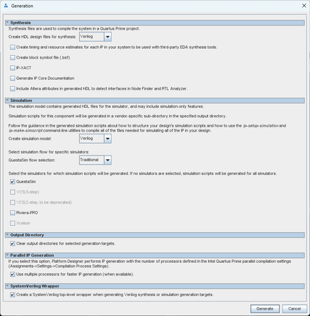
Hello, I'm unable to generate a simple PLL IP on a particular Win 11 machine. It works fine on a different Win 11 machine. Below is a partial log that shows the error. Note that I replaced my own user name with <username> below. Info: Starting: Create HDL design files for synthesis Info: qsys-generate C:\Projects\fw_ml_module_local\ip\pll_io.ip --synthesis=VERILOG --output-directory=C:\Projects\fw_ml_module_local\ip\pll_io --family="Agilex 3" --part=A3CY050BB18AI6S Info: pll_io.iopll_0: Able to implement PLL with user settings Info: pll_io: "Transforming system: pll_io" Info: pll_io: "Naming system components in system: pll_io" Info: pll_io: "Processing generation queue" Info: pll_io: "Generating: pll_io" Info: pll_io: "Generating: pll_io_altera_iopll_2110_txusefy" Error: add_fileset_file: No such file C:/altera_pro/26.1/ip/altera/altera_iopll/top/{C:/Users/<username>/AppData/Local/Temp/alt0637_15290807326924327962.dir/0003_iopll_0_gen/altera_falconmesa_ph2_iopll.sdc} while executing "add_fileset_file ${output_name}.sdc SDC_ENTITY PATH $sdc_file {NO_AUTO_INSTANCE_DISCOVERY NO_SDC_PROMOTION READ_DURING_POST_SYN_AND_POST_FIT_TIMING_AN..." (procedure "generate_sdc_related_files" line 560) invoked from within "generate_sdc_related_files $tmpdir $name " (procedure "generate_sdcs_and_mif" line 24) invoked from within "generate_sdcs_and_mif $name" (procedure "generate_synth_falconmesa_ph2" line 12) invoked from within "generate_synth_falconmesa_ph2 $name" (procedure "generate_synth" line 9) invoked from within "generate_synth pll_io_altera_iopll_2110_txusefy" Info: pll_io: Done "pll_io" with 2 modules, 4 files Info: Finished: Create HDL design files for synthesis Info: Generation of C:/Projects/fw_ml_module_local/ip/pll_io.ip (pll_io) took 9192 ms When I run the same PLL generation on a different Win 11 machine, I don't see mention of add_fileset_file in the log. Below are the Generation settings.Solved182Views0likes11Commentsavalon MM generator read issue
I'm using avalon MM BFM to stimuli my slave avalon interface, however, when doing u_avalon_MM_gen.mm_master_bfm_0.set_command_address(addr); u_avalon_MM_gen.mm_master_bfm_0.set_command_byte_enable(4'hF, 0); u_avalon_MM_gen.mm_master_bfm_0.set_command_request(REQ_READ); u_avalon_MM_gen.mm_master_bfm_0.push_command(); @(u_avalon_MM_gen.mm_master_bfm_0.signal_read_response_complete); data = u_avalon_MM_gen.mm_master_bfm_0.get_response_data(0); $display("[%0t] READ Addr=0x%08h Data=0x%08h", $time, addr, data); the data seem delay by 1 register transaction eg. READ addr=0 data=0 READ addr=4 data=1020001 <- this data should be at addr=0, but get_response_data(0) pop on the next addr return.data (get_response_data) has 3 ns delay from rising clock edge or from complete.data change90Views0likes6Comments