interfaces
346 Topics
Why does the Quartus® Prime Pro Edition Software version 26.1 complete compilation even when two PCIe* Hard IPs are enabled for CvP application?
Description Due to a problem in the Quartus® Prime Pro Edition software version 26.1 and earlier, compilation may complete successfully when more than one PCIe* IP is enabled for CvP application, which conflicts with the description in the Configuration via Protocol (CvP) Implementation User Guide. Resolution Currently, there is no workaround. This problem is scheduled to be fixed in a future release of the Quartus Prime Pro Edition software.47Views0likes0CommentsWhy does the Agilex® 5 DisplayPort SST TX-Only example design fail to generate when AXIS-VVP Full is enabled?
Description Due to a problem in the Quartus® Prime Pro Edition Software version 25.3 and earlier, you might see the following example design generation errors when generating the Agilex® 5 DisplayPort SST TX-Only example design with AXIS-VVP Full enabled. error: 'VVP_TPG_BASE' undeclared (first use in this function) Error: Failed to generate example design example_design to: <example_design_path> Resolution This problem is scheduled to be fixed in a future release of the Quartus Prime Pro Edition Software.47Views0likes0CommentsWhy does the Quartus® Prime Pro Edition Software report a pin placement error when Customize Pin Selections is disabled in the LVDS SERDES IP?
Description When using the LVDS SERDES IP with Agilex® 5 FPGAs or Agilex® FPGA 7 M-Series FPGAs, the physical byte and pin assignment must match the pin index specified under the Pin Settings tab in the IP Catalog GUI. If a physical byte or pin is selected without matching the corresponding pin index, the Quartus® Prime Pro Edition Software may report a pin-placement or compilation error. Even when Customize Pin Selections is not selected, each pin must be assigned according to the default byte and pin values specified for its corresponding pin index in the Pin Settings tab. Not selecting this option does not allow arbitrary byte or pin assignments. To use a different byte and pin assignment, select Customize Pin Selections and manually assign the byte and pin locations according to the design requirements and the supported device pin mapping. Resolution To avoid this problem, assign the LVDS SERDES IP pins according to the specified pin index in the Pin Settings tab; to use a different byte and pin assignment, select Customize Pin Selections and manually assign the byte and pin locations according to the design requirements.79Views0likes0CommentsHow do I retarget the F-Tile Ethernet Hard IP 100G example design from the Agilex® 7 FPGA I-Series Development Kit QSFP-DD J27 (QSFPDD0) to the Agilex® 7 FPGA M-Series Development Kit QSFP-DD J16 (QSFPDD CONN0)?
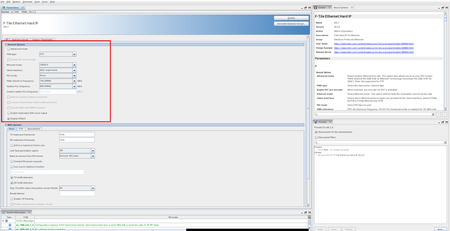
Description Currently, the F-Tile Ethernet Hard IP GUI only has the option to generate the 100GE-4 example design that targets the Agilex® 7 FPGA I-Series Development Kit QSFP-DD connector J27 (QSFPDD0). There is no way for users to generate a 100GE-4 F-tile Ethernet Hard IP example design through the IP GUI that maps the IP directly to QSFP-DD connector J16 (QSFPDD CONN0) on the Agilex® 7 FPGA M-Series Development Kit (DK-DEV-AGM039EA). For users working on the Agilex 7 FPGA M-Series devkit, this creates additional work for the users to refer to the Agilex 7 FPGA M-Series board schematics to modify the pin assignments and other SDM/Power Management settings accordingly to create an FPGA image that is compatible with the M-Series devkit. With the steps specified below, users can now modify the devkit agnostic 100GE-4 example design to map to the Agilex 7 FPGA M-Series Development Kit’s J16 QSFP-DD connector (QSFPDD CONN0) by generating the example design using the IP GUI with Select Board set to None, then retarget the Quartus® Settings File (.qsf) pin, I/O standard, and board power-management assignments to the DK-DEV-AGM039EA J16 pinout, and then recompile to generate the FPGA image, by following the steps specified below. Resolution To obtain the 100GE-4 F-Tile Ethernet Hard IP example design in the Quartus® Prime Pro Edition Software that maps to Agilex 7 FPGA M-Series Development Kit (DK-DEV-AGM039EA) on J16 (QSFPDD CONN0) port, follow these steps: Open the F-Tile Ethernet Hard IP Parameter Editor and set General Options as follows (see attached screenshot): PMA type FGT; Ethernet mode 100GE-4; Client interface MAC segmented; FEC mode None; PMA reference frequency 156.250000 MHz; System PLL frequency 805.664062 MHz. Open the Example Design tab and set Select Board to None; Select device initialization clock to OSC_CLK_1_125MHZ. Click Generate Example Design to generate the ED. Edit the example design .qsf so board-level assignments match the Agilex 7 M-Series Development Kit QSFP-DD J16 (QSFPDD CONN0). Compare the originally generated .qsf (left) to the retargeted .qsf (right) in the attached screenshots. Apply pin/location, fitter/assembler power-management, and ENTITY(eth_f_hw) I/O standard / virtual-pin changes as shown in these screenshots. Save the .qsf and run a full compile to generate the .sof. Program the DK-DEV-AGM039EA board and confirm loopback link-up on J16 QSFP port by connecting the external loopback module as seen below. Additional Information Source APS: 01009271 (Closed). Related engineering AR: QS-615224. RAE validated the retargeted design on DK-DEV-AGM039EA before delivering a reference QAR.58Views0likes0CommentsWhy does the Quartus® Prime Pro Edition Software report that no IOPLL is available when placing the Low Latency E-Tile 40G Ethernet FPGA IP in an HPS shared GPIO Bank?
Description Due to a clocking limitation of HPS Shared GPIO Bank, the Low Latency E-Tile 40G Ethernet FPGA IP cannot be placed in an HPS Shared GPIO Bank when a design targets Agilex® 7 FPGA F-Series. If the IP placement requires its IOPLLs to use an HPS Shared GPIO Bank, the fitter may report that no IOPLL IP is available and compilation may fail during the fitter stage. The Low Latency E-Tile 40G Ethernet FPGA IP uses IOPLL IPs configured in Normal Compensation mode. However, the IOPLL resources in an HPS Shared GPIO Bank support Direct Compensation mode only. Consequently, the fitter cannot legally place the IOPLLs in the Low Latency E-tile 40G Ethernet FPGA IP in an HPS Shared GPIO Bank. Resolution To avoid this problem, place the Low Latency E-Tile 40G Ethernet FPGA IP in a supported non-HPS Shared GPIO Bank.95Views0likes0CommentsWhy does the Quartus® Prime Pro fitter fail when compiling the Agilex® 5 GTS HDMI IP Clocked Video design example with the HDMI PHY?
Description Due to a problem in the Quartus® Prime Pro Edition Software version 26.1.1, the fitter may fail during placement when compiling the Agilex® 5 GTS HDMI IP design example configured with the Clocked Video interface with the HDMI PHY configuration. The failure occurs while routing a core global signal for the HDMI receive path and reports that no valid lab location can be found near chip coordinates (157, 74). The fitter then exits unsuccessfully. Resolution This problem will be fixed in a future release of the Quartus Prime Pro Edition Software.57Views0likes0CommentsWhy isn't the Debug Toolkit using AXI Streaming IP for PCIe* with F-Tile variant shown in the System Console window when using the Quartus® Prime Pro Edition software version 25.3 and 25.3.1 ?
Description Due to a problem in the Quartus® Prime Pro Edition software version 25.3 and 25.3.1, the Debug Toolkit using AXI Streaming IP for PCIe* with F-Tile variant isn't shown in the System Console window. Resolution A patch is available to fix this problem for the Quartus Prime Pro Edition software versions 25.3. Download and install patch 0.37 below. This problem is fixed beginning with the Quartus Prime Pro Edition software version 26.1.32Views0likes0CommentsWhy does the Low Latency 40G Ethernet IP drop non-PTP packets when PTP residence-time update is enabled?
Description Due to a problem in the Quartus® Standard Edition software version 21.1, you may see the Low Latency 40G Ethernet IP may drop large non-PTP packets when the tx_etstamp_ins_ctrl_residence_time_update (PTP residence-time update) is asserted. This problem is typically observed with jumbo frames of approximately 3000 bytes or larger. The affected packets may be counted at the RX interface but may not appear at the TX output. PTP packets themselves may continue to transmit correctly. This problem is not observed when tx_etstamp_ins_ctrl_residence_time_update (PTP residence-time update) is kept deasserted. Resolution A patch (21.1std patch 0.16std) is available to fix this problem for the Quartus Standard Edition Software version 21.1. To request the patch, contact your local Altera support representative. This problem is resolved in the Quartus Prime Pro Edition Software 26.1. Altera recommends migrating to the latest Quartus Prime Pro Edition Software to address this problem.61Views0likes0CommentsWhy do I see this warning message after enabled Transceiver Toolkit Debugging Features in GTS SDI II Serial Loopback Design Example?
Description Due to a problem in the Quartus® Prime Pro Edition software version 26.1.1, you will observe below. “warning check failed! > warning: no path is found satisfying assignment" “set_max_skew -from get_registers auto_fab_0|alt_sld_fab_0|alt_sld_fab_0|stfabric|h2t1_fifo|in_wr_ptr_gray -to get_registers auto_fab_0|alt_sld_fab_0|alt_sld_fab_0|stfabric|h2t1_fifo|write_crosser|sync.u|din_s1 -get_skew_value_from_clock_period src_clock_period -skew_value_multiplier 0.800 - This assignment will be ignored.” It happens when user enables the Transceiver Toolkit Debugging Features in GTS SDI II Serial Loopback Design Example. This problem happens due to the undefined path of the dc_fifo.sdc. Resolution This problem is scheduled to be fixed in a future release of Quartus Prime Pro Edition software.72Views0likes0CommentsWhy am I seeing High Severity DA warning: "Multiple Clock Domains Driving a Synchronizer Chain" after enabled Transceiver Toolkit in Dual-Simplex Parallel loopback Design Example?
Description Due to a problem in the Quartus® Prime Pro Edition software version 26.1.1, you may see a DA warning: "Multiple Clock Domains Driving a Synchronizer Chain" in the compilation report for the GTS SDI II Dual-Simplex Parallel Loopback design example when the transceiver toolkit is enabled. Resolution This DA Warning can be ignored in 26.1.1, and this problem is scheduled to be fixed in a future release of Quartus Prime Pro Edition software.63Views0likes0Comments