core logic
87 Topics
DK-DEV-AGI027RBES CXL Type-3 example remains in reset and is not detected by host
Hi, I have several Agilex 7 FPGA I-Series Development Kits with serial numbers 8100035 and 8020138. My goal is to run the boards as CXL Type-3 devices and verify that they can be enumerated by the host. I am currently debugging board 8020138 with the following setup: Board: DK-DEV-AGI027RBES FPGA: AGIB027R29A1E2VR3 Power configuration: Power Solution 2 Quartus Prime Pro: 24.3 Connection: PCIe edge connector Design: CXL Type 3 with DDR4 Link width: CXL x16 Number of slices: 2 PLD clock: 400 MHz Reference clock mode: Common Refclk source is global clock: Enabled The board can successfully enumerate as a normal PCIe endpoint when using the pcie_ed example design included in: agilex_agib027r29a1e1vb_fpga_revc_v24.3b194_v1.1 However, when I generate and compile the RBES CXL Type-3 DDR4 example design, the host cannot detect the device and it does not appear in lspci. I added JTAG debug registers and Signal Tap probes. The observed status is: config_done = 1 pll_lock = 1 sip_rst_n = 0 cxl_warm_rst_n = 0 cxl_cold_rst_n = 0 ip2hdm_reset_n = 0 ip2cafu_avmm_rstn = 0 ip2csr_avmm_rstn = 0 pf0_bus_master_en = 0 pf0_memory_access_en = 0 pf0_msix_enable = 0 The fabric heartbeat counter(refclk4) is running, so FPGA configuration and the debug fabric clock are working. However, the CXL cold, warm, and SIP resets never deassert, and host enumeration never starts. Could you please confirm: Are these CXL IP settings correct for board 8020138, Power Solution 2, and the PCIe edge connector? For CXL x16 with two slices, must both refclk0 and refclk1 be active? What conditions control cxl_cold_rst_n, cxl_warm_rst_n, and sip_warm_rstn_o? How can I observe the physical PERST# status, R-Tile reset status, PHY initialization status, LTSSM state, and link-up status? Should Enable PIPE Mode Simulation be disabled for hardware operation? Is 400 MHz the correct PLD clock frequency? Is there a known-good CXL Type-3 DDR4 example project or SOF for DK-DEV-AGI027RBES with FPGA AGIB027R29A1E2VR3? Are there any required Quartus 24.3 patches for this board and CXL IP? The normal PCIe example works, but the CXL example remains in reset. This suggests the issue may be related to the CXL IP configuration, reference-clock/reset requirements, or the generated example-design constraints. I can provide the IP configuration, QSF/SDC files, Signal Tap captures, compilation logs, and host logs if needed. Thank you. Best regards, Jeffrey56Views0likes4Comments
Three 9x9 multipliers in one DSP
Hello everyone, Do have somebody the project example with three 9x9 multipliers in one DSP looks like in this post: How to configure DSP block in "three 9x9 multipliers" mode? | Altera Community - 90399 I tired to do this project and I have got one mult. per DSP.36Views0likes1Comment
The DC_FIFO issue of Cyclone 10 GX devices
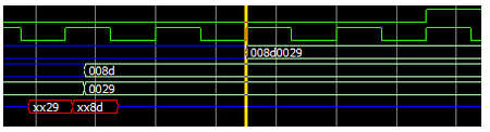
Hello Guys, We are using 10CX220F780 and 10CX105F780 devices now. They are communicating thru XCVR. So one DC_FIFO is realized between RX received data and user logic fabric. This DC FIFO operation always has problem during the first operating. But it will be normal during the second operating. As the above image indicates, RX get data from XCVR and put them to FIFO. The write is ok, however, the reading has problem. Because the first read data is ZERO, this causes the following reads all halt. I apply one more same operation, now it's ok, as following image: As above image indicates, one data is put into FIFO, and it will be read out from this FIFO in time. But why always the first time operating is not correct after power-up or re-configuring FPGA? I did one test: FIFO's Rdreq is fix to high level. Then I got the following result: As above image indicates, the first data x"40000000" can't be written into FIFO. So I always got ZERO for the first data. Buy how this can happen? I kept detecting more deeply, as following image As above image indicates, after Wreq valid, 2 clock cycles later, Usedw will change, and 2 more clock cycles later, empty signal will be changed to low level. This is the problem. Usedw and empty signals are changed too fast. I checked normal timing, UsedW should be changed 3 clock cycles later after Wreq valid, and empty should be changed 5 clock cycles later after Wreq valid. Why can this happen? And always happen one time after power-up. Best Regard735Views0likes8Comments
Cyclone 10 GX AS x4 Configuration Compatibility with Infineon S25FS512S (Custom Flash Definition)
We are trying to use the Infineon S25FS512S QSPI NOR Flash with Cyclone 10 GX in Active Serial x4 (AS x4) configuration by creating a Custom Flash Definition based on AN229767. JTAG programming completes successfully, but FPGA configuration fails in AS x4 mode. We have performed extensive debugging and would like to understand whether this is a supported use case or if there are any known limitations. Observations Flash Programming JTAG programming completes successfully. Flash verification completes successfully. Configuration Behavior Active Serial x1 configuration works correctly. Active Serial x4 configuration fails. The FPGA successfully issues the RDID (0x9F) command. The FPGA then attempts to read the Boot Information from address 0x00000000. Logic Analyzer Observation During AS x4 configuration, the FPGA issues the EBh (Quad I/O Read) command. According to the Infineon S25FS512S datasheet, the expected transaction is: EBh → 4-byte Address → Mode Byte (8 bits) → Dummy Cycles → Data However, the captured waveform shows: EBh → 4-byte Address → Dummy Cycles → Data No Mode Byte is observed between the address and dummy cycles. Based on the S25FS512S command protocol, this could cause the flash to interpret the transaction differently and return misaligned data. We would like Altera to confirm whether this behavior is expected from the Cyclone 10 GX configuration controller. Additional Information We reviewed AN229767, but could not find any mechanism in the Custom Flash Definition to configure or insert the Mode Byte required by the EBh command. We also observed that the Custom Flash Definition supports Read Register commands only for fixed register opcodes and does not appear to support RDAR (0x65) with a register address. Questions Does the Cyclone 10 GX configuration controller support transmitting the mandatory Mode Byte required by the EBh (Quad I/O Read) command? If not, is this a known limitation of the Cyclone 10 GX configuration controller or Quartus Programmer? Is there any supported method to modify the Quad I/O Read command sequence in the Custom Flash Definition? Has Altera validated any Custom Flash Definition for the S25FS512S that can be shared as a reference? Environment FPGA: Cyclone 10 GX Flash: Infineon S25FS512S Configuration Mode: Active Serial x1 (working), Active Serial x4 (failing) Programming Method: Quartus Programmer using a Custom Flash Definition based on AN229767 We would appreciate any guidance, clarification, or a reference implementation for using the S25FS512S with Cyclone 10 GX in Active Serial x4 mode.904Views0likes14Comments
FPGA simulation and real HW behavior discrepancy
Dear Altera Quartus 18.1 sim lib could try 20.1 or newer but not sure this is due to Quartus version as it is sim lib. I am encounter an unexplainable experiment result that contradicts simulation and real HW. Background when interfacing a DQS DQ readout a IDDR with CCD sync flops are used. For these primitives, it should expected 1 + 2 and clock +ve edge should expect data push out. [A] This can simply considered as early push out but it should not act as such. With the use of "__ALTERA_STD__METASTABLE_SIM" we expected some metastable on the output. [B] Now things are more reasonable where 2 +ve clocks are expected. If we consider a full data w/o xx, things become unrecognizable. [C] The most interesting part when apply on real HW, it do produce correct data and the latencies do obeyed. altddio_in#( .intended_device_family ( "Cyclone IV E" ), .invert_input_clocks ( "ON" ), .lpm_hint ( "UNUSED" ), .lpm_type ( "altddio_in" ), .power_up_high ( "OFF" ), .width ( 8 ) )ddi_d_l( .aclr (reset), .datain (foo[7:0]), .inclock (bar[0]), .dataout_h (foobar_h[0+:8]), .dataout_l (foobar_l[0+:8]), .aset (1'b0), .inclocken (1'b1), .sclr (1'b0), .sset (1'b0) ); + altera_std_synchronizer_bundle#( .width (foobar_bw *2), .depth (2) )async_flops( .clk (clock), .reset_n (~reset), .din (foobar), .dout (foobar_ccd) );107Views0likes1Comment
Introducing the Altera Community AI Responder — Beta
Altera is introducing the AI Responder, an assistant built into the Altera Community to help provide faster, context-aware guidance for Altera product questions. It uses relevant public Altera documentation and Knowledge Database content, with coverage continuing to expand. The AI Responder may provide source references and can hand off complex or out-of-scope questions to an Altera subject-matter expert. As a beta feature, responses may contain errors or omissions, so please review the sources and verify technical guidance against official Altera documentation before implementation. If the response does not fully address your question, add more context and tag ai_responder to continue the discussion. We welcome your feedback as we improve the Community experience.41Views0likes0CommentsQuartus Programmer 21.1: JTAG Server Error Code 82 – Port 1309 Cannot Be Bound
Hello Altera Community, I am working on an FPGA project using a Cyclone IV FPGA development board and an Altera USB-Blaster. I am currently unable to program the FPGA because Quartus Programmer cannot access the JTAG server. System details: - OS: Windows 11 64-bit - Software: Quartus Programmer 21.1 - Installation path: C:\intelFPGA\21.1\qprogrammer - Programmer: Altera USB-Blaster - FPGA: Cyclone IV development board The USB-Blaster is detected by Windows Device Manager and the driver is installed. The USB-Blaster also powers on normally. However, Quartus Programmer gives: "Attempted to access JTAG server -- internal error code 82 occurred" When I run: jtagconfig I get: Error when scanning hardware - Server error Sometimes it also hangs at: Connecting to server(s) [...] I checked the JTAG server using: jtagserver --status It reports: Installed JTAG server is 'C:\intelFPGA\21.1\qprogrammer\bin64\jtagserver.exe' Server is stopped Remote clients are disabled I tried reinstalling the JTAG server: jtagserver --install jtagserver --start But the server immediately stops. I also tried: net start "Altera JTAG Server" The result was: The Altera JTAG Server service could not be started. The service did not report an error. NET HELPMSG 3534. I then ran: jtagserver.exe --foreground and received: Unable to bind changedetect socket: 10048 Can't bind to TCP port 1309 - exiting I checked the port using: netstat -ano | findstr 1309 and found that TCP port 1309 was being used/listened to by another process, for example PID 12888. I tried terminating the process using: taskkill /F /PID 12888 but Windows reported: ERROR: The process with PID 12888 could not be terminated. Reason: There is no running instance of the task. I also tried stopping the JTAG server, reinstalling it, and restarting it. In addition, I already tried the following: 1. Disabled PCI Express → Link State Power Management. 2. Disabled USB Root Hub power saving ("Allow the computer to turn off this device to save power"). 3. Stopped the Print Spooler service. 4. Closed Quartus/Programmer-related applications. 5. Reinstalled the JTAG Server. 6. Restarted the computer. 7. Tried starting the JTAG server manually. 8. Checked TCP port 1309 using netstat. The problem still remains. My main questions are: 1. Why is Quartus Programmer 21.1 unable to start the JTAG Server? 2. What is causing TCP port 1309 to remain occupied? 3. Is there a known issue with Quartus Programmer 21.1 and Windows 11? 4. Is there a recommended patch, driver, or newer Quartus Programmer version for this problem? 5. Is it possible to configure the JTAG server to use another TCP port? 6. What is the correct way to completely remove and reinstall the JTAG Server on Windows 11? 7. Is there anything else I should check before reinstalling Quartus Programmer? I would appreciate any guidance on how to get the JTAG Server running so that jtagconfig can detect my USB-Blaster and FPGA. Thank you.278Views0likes5Comments
Updated .brd file for Stratix 10 GX dev kit
Referencing this post: EK-10M08E144 PCB .brd file corrupted | Altera Community - 302242 The .brd file that comes in the documentation at: https://www.altera.com/products/devkit/po-3028/stratix-10-gx-signal-integrity-development-kit-h-tile ...was done in Allegro, prior to version 16.6. The only available Allegro viewer gives an error because it was done prior to version 16.6, and you need the DB Doctor utility to update the file. The only way to get the DB Doctor utility is to install Allegro. If I had Allegro...I would not be installing the Allegro viewer. Altera: As mentioned in the post above (well over a year ago), it would make sense for you to update your files so customers can view the board of their $10K+ development board. How do we make that happen? Thanks!532Views0likes4Comments
8 port 10/25G ethernet interface in Stratix 10
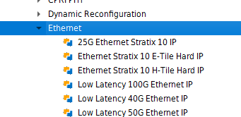
We have custom board made with Stratix 10 1ST085EN2F43I2LG. The board has 8 SFP28 ports the needs to talk to 10/25G ethernet devices. This board is used to test the connected devices by sending a fixed Ethernet packets and analyse the received Ethernet packets. The SFP ports needs to be selectable between 10G and 25G and enable/Disable RS-FEC. Also need the MAC statistics registers and PTP timestamping. We could see two different IP cores available for this in the IP catalogue, 25G Ethernet Stratix 10 IP, and Ethernet Stratix 10 E-Tile Hard IP. Which one is the right IP for this requirement.692Views0likes9Comments