Forum Discussion

 New Contributor
Strange issues on FPGA
 New Contributor
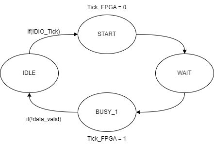
Let me explain the process of this FPGA:
- IDLE: After receiving the DIO_Tick signal, it transitions to the START state.
- START: It sends a low-level Tick_FPGA signal, then enters a delay state (originally using a counter), and transitions to the BUSY state.
- BUSY: It returns the Tick_FPGA signal to high level and waits for the data_valid signal, before going back to IDLE.
(CNVST, BUSY, CS, SCK, and DATA are mainly used to confirm whether the local side has received the Tick_FPGA signal and can be ignored.)
The following is the correct timing:
(This data_valid signal has been modified in both sending and receiving)
@anonimcs wrote:Hi,
Firstly, could you add the snippets a bit close-up ? It's really hard to see the details, therefore to debug. Regarding the issues:
1) If the Tick_FPGA is staying low, your FSM might be stuck at the IDLE state, waiting for Dio_tick. In the second snippet I see that there's a rapid transition of Dio_tick to 0 and then back to 1, maybe this transition happens when the FSM is not in the IDLE state but in another state. But since there's no state signal in the waveforms, I cannot be sure. Maybe you can add that one and the counter signals to the waveform ?
It encounters two issues:
1. Tick_FPGA cannot return to a high level:
Overview of the timing diagram:
Zoom In(LEDs to IO to observe the state):
Here, the Tick_FPGA signal suddenly goes low.
According to the FSM's LEDs I set for each state, it has jump to an illegal state.
2. FPGA does not correctly receive data_valid
It can be seen that the preceding timing is correct, but sometimes data_valid is not received, causing the FPGA to get stuck.
According to the FSM's LED indicators, it is stuck in the BUSY state waiting for data_valid.
I have tried adding synchronization to wait for the external signal to stabilize, but it seems to not resolve the issue:
		data_valid_sync1 <= data_valid;
		data_valid_sync2 <= data_valid_sync1;
@anonimcs wrote:2) What is DATA in A4 ? data_in or data_out ? If it's data_in, it could be the same as 1), getting the data_valid transition to 0 in another state. But if it's data_out, it should be stuck in the BUSY_1 state indeed, but that shouldn't be the case given that the data_valid is wide enough for the clock to catch.
My idea is that you're stuck at the reset state for the most of the time, and when it's out of that, the FSM barely has time to do anything (I assume A4 is data_in)
-> I'm sorry for the confusion. DATA is the signal sent by this FPGA to another FPGA using the Tick_FPGA signal to drive the ADC's SPI DATA.
This FPGA's data is transmitted in parallel (originally, I intended to use serial, but the code I wrote didn't meet expectations; that's another issue). Due to the large number of channels required for 12 bits, I used SPI's DATA for confirmation.
	input wire [11:0] data_in,
	output reg [11:0] data_out,
I really can't find a way to solve these two problems, so I'm hoping to get some help.

 Super Contributor
Hi,
we see that unexpected state enters on DIO_Tick edge. Where is this signal originated? Guess it's also asynchronous and needs synchronization.
- Scarlet2 years ago
@FvM wrote:Hi,
we see that unexpected state enters on DIO_Tick edge. Where is this signal originated? Guess it's also asynchronous and needs synchronization.DIO_Tick comes from the DIO card of the PC.
I found that both of these issues may stem from errors in receiving external signals. I suspect that the data_valid is causing the FSM to jump to an illegal state, leading to the incorrect Tick_FPGA signal.
In designing the FPGA to receive external signals, I'm not experienced enough, which has led to unexpected errors even in simple state machines.
Currently, I have resolved the timing issues related to external signal processing.


