Forum Discussion

Altera_Forum's avatar
Altera_Forum
Icon for Honored Contributor rankHonored Contributor
14 years ago

Please help me with setup slack error

Hi:

I use FPGA to capture 6 channel ADC output simutaneously. The pin of ADC output clock is COUT and 8MHz. The width of ADC output data is 16 bits. The time of valid data is about half of the period of COUT, that is, 62.5 ns. The relation between COUT and DAB( pin name of output data) is as follows:

https://www.alteraforum.com/forum/attachment.php?attachmentid=3899

the timing specification of ADC is as follows:

https://www.alteraforum.com/forum/attachment.php?attachmentid=3900

I use the following commands to constrain the source-synchronous input:

--- Quote Start ---

# base clock, 90 degree phase shift

create_clock -name {adc_cout} -period 125.000 -waveform { 31.250 93.750 } [get_ports { ADC3_COUT ADC2_COUT ADC1_COUT }]

# virtual clock, for set_input_delay

create_clock -name {adc_virt_cout} -period 125.000 -waveform { 0.000 62.500 }

# set input delay

set_input_delay -add_delay -max -clock [get_clocks {adc_virt_cout}] 54.500 [get_ports {ADC1_DA[0]}]

set_input_delay -add_delay -min -clock [get_clocks {adc_virt_cout}] 2.000 [get_ports {ADC1_DA[0]}]

set_input_delay -add_delay -max -clock [get_clocks {adc_virt_cout}] 54.500 [get_ports {ADC1_DA[1]}]

set_input_delay -add_delay -min -clock [get_clocks {adc_virt_cout}] 2.000 [get_ports {ADC1_DA[1]}]

...

--- Quote End ---

After reporting timing, the setup slack is:

https://www.alteraforum.com/forum/attachment.php?attachmentid=3901

the hold slack is:

https://www.alteraforum.com/forum/attachment.php?attachmentid=3902

I still couldn't figure out what went wrong. Could anyone please help me? Thanks!
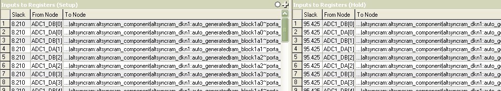
6 Replies

  • Altera_Forum's avatar
    Altera_Forum
    Icon for Honored Contributor rankHonored Contributor

    I understand you have three ADC clocks each at 8MHz then I will try this:

    Assuming tCO = half clock period, you may lower min values to say 62.0

    create_clock -name {adc1_cout} -period 125.000 [get_ports {ADC1_COUT }]

    create_clock -name {adc2_cout} -period 125.000 [get_ports {ADC2_COUT }]

    create_clock -name {adc3_cout} -period 125.000 [get_ports {ADC3_COUT }]

    set_input_delay -max -clock [get_clocks {adc1_cout}] 62.5 [get_ports {ADC1_DA

    [*]}]

    set_input_delay -add_delay -min -clock [get_clocks {adc1_cout}] 62.5 [get_ports {ADC1_DA

    [*]}]

    set_input_delay -max -clock [get_clocks {adc2_cout}] 62.5 [get_ports {ADC2_DA

    [*]}]

    set_input_delay -add_delay -min -clock [get_clocks {adc2_cout}] 62.5 [get_ports {ADC2_DA

    [*]}]

    set_input_delay delay -max -clock [get_clocks {adc3_cout}] 62.5 [get_ports {ADC3_DA

    [*]}]

    set_input_delay -add_delay -min -clock [get_clocks {adc3_cout}] 62.5 [get_ports {ADC3_DA

    [*]}]

  • Altera_Forum's avatar
    Altera_Forum
    Icon for Honored Contributor rankHonored Contributor

    Thank you very much for your reply, kaz!

    --- Quote Start ---

    I understand you have three ADC clocks each at 8MH

    --- Quote End ---

    This is exactly what I meant.

    --- Quote Start ---

    create_clock -name {adc1_cout} -period 125.000 [get_ports {ADC1_COUT }]

    create_clock -name {adc2_cout} -period 125.000 [get_ports {ADC2_COUT }]

    create_clock -name {adc3_cout} -period 125.000 [get_ports {ADC3_COUT }]

    --- Quote End ---

    I am not convinced if three ADCs' output will come out at the same time, so this may produce better timing.

    Also, I went through the AN433 and found a method using virtual clock to constrain the design(I will definitely split "adc_virt_cout" into three virtual clocks later. :) ):

    --- Quote Start ---

    set_input_delay -add_delay -max -clock [get_clocks {adc_virt_cout}] 23.250 [get_ports {ADC1_DA[0]}]

    set_input_delay -add_delay -min -clock [get_clocks {adc_virt_cout}] 2.000 [get_ports {ADC1_DA[0]}]

    set_input_delay -add_delay -max -clock [get_clocks {adc_virt_cout}] 23.250 [get_ports {ADC1_DA[1]}]

    set_input_delay -add_delay -min -clock [get_clocks {adc_virt_cout}] 2.000 [get_ports {ADC1_DA[1]}]

    --- Quote End ---

    This considers the setup and hold relationships are not the same as they are with respect to the input clock. The input data is edge-aligned with respect to the virtual clock. The hold

    requirement with respect to the virtual clock must decrease by the amount of the shift

    (period/4 for a center-aligned DDR interface). The setup requirement with respect to

    the virtual clock must increase by the amount of the shift (period/4 for a

    center-aligned DDR interface). The input maximum and minimum delay values both

    decrease by the amount of the shift (period/4 for a center-aligned DDR interface).

    the period here is 125ns, divided by 4 is 31.25ns. ADC data output have setup timing of 8ns, so the input maximum delay is 62.5 - 31.25 - 8 = 23.25ns. I reserve the hold timing of 2ns. This produce the follwing timing report:

    https://www.alteraforum.com/forum/attachment.php?attachmentid=3904

    The setup slack is 8.21ns. This slack should represent the estimation of setup time generated by TimeQuest. What brings the variation between the setup slack and ADC setup time?
  • Altera_Forum's avatar
    Altera_Forum
    Icon for Honored Contributor rankHonored Contributor

    If your interface is DDR then you need further additions for falling edges.

    see Timequest resource centre on altera.com

    With regard to 8 ns setup time of ADC, I am not sure what you mean because ADC is an outputting device, only its tCO matters.

    May be you mean maximum/minimum tCO or skew at ADC output, in that case it is fair enough to use that figure as range diff between max/min.
  • Altera_Forum's avatar
    Altera_Forum
    Icon for Honored Contributor rankHonored Contributor

    Hi, kaz:

    Thank you for pointing out the problem.

    According the ADC's datasheet, the maximum tCO is 9 ns with respect to ADC_CLK falling edge(ADC_CLK is the sample clock of ADC). The minimum tH(Output hold time from COUT to data invalid) is 2 ns, and the minimum tSU(Output hold time from COUT or COUT to data invalid) is 8 ns, both with respect to COUT rising edge(COUT is the latch clock for ADC's data outputs).

    The datasheet recommends "Data out should be referenced to COUT", while it also says "The relationship between ADC_CLK and COUT is not fixed and depends on the power-on conditions".

    From the recommendation of ADC datasheet, I think the relationship between COUT and tCO is not fixed. In other words, tCO varies in different power-on conditions. So tCO may be useless for the input delay constraints. That's why I refered to setup and hold timing of ADC output in my thread. Now I have no idea how to constrain my design. Can you give me some enlightment? Thanks in advance!
  • Altera_Forum's avatar
    Altera_Forum
    Icon for Honored Contributor rankHonored Contributor

    I am still not convinced by referring to tSU/tH of an outputting device. These are parameters that apply to inputting device(fpga in your case). It could be what ADC recommends for the receiving device.

    A variable tCO would mean skew and that will be evident on min/max tCO or min/max recommended tSU/tH
  • Altera_Forum's avatar
    Altera_Forum
    Icon for Honored Contributor rankHonored Contributor

    Thank you for the reply.

    I decide to use the tCO anyway. Maybe a little risky, but we will change the constraints based on practical result.

    Thanks again for your help!