Forum Discussion

 Occasional Contributor
Unable to scan JTAG chain, TCK only 2V
I have trouble with some development board with 10CL006YE144G. While the configuation by JTAG worked a while, the FPGA is no longer recognized by the programmer using Autodetect.
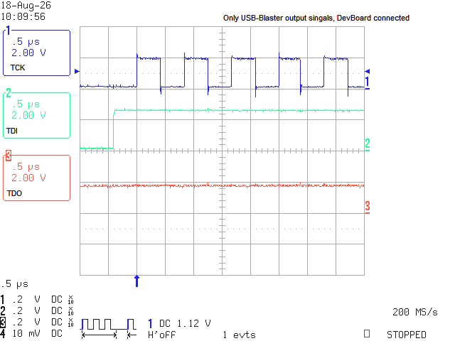
I checked the voltages of signals and while the power supply (JTAG Header Pin 4) is stable 2.5V, the TCK signal is only driven to 2V High level. As all I/Os are driven by 3.3V, I assume the 2V is not or at least no stable high signal. As two USB Blasters do not work / work on other designs and with the signal is 2.5V w/o connected development board. I'm afraeid the FPGA I/O is broken...
Unfortunately, the dev-Board lacks protection devices (direct connection header to Pin, no protection diodes). I assume connecting the USB-Blaster being referenced to the PC to the board being referenced to board's power supply could cause voltages spikes on the interface overloading and damaging the FPGA :-(
Is this a keep the board simple and cheap, i.e. not even a series resistor, trap?
Thanks in advance and KR Carlhermann
Hello Carlhermann,
Thank you for the detailed testing. Your standalone test confirms that the voltage drop is caused by the older USB-Blaster cable rather than the FPGA or development board.
A 2.5 V target supply and the 1 kΩ TCK pull-down are supported connections. However, older USB-Blaster hardware revisions used a different MAX3378-based output circuit, while later revisions added buffering. The failing cable therefore appears to have insufficient output-drive margin or may be degraded; this does not indicate that the FPGA is damaged.
Please continue using the known-good cable. No board modification should be required, and we can consider this issue resolved.
Best regards,
Fakhrul
4 Replies
 FakhrulA_altera
Regular Contributor
Hello Carlhermann,
Thank you for the detailed testing. Your standalone test confirms that the voltage drop is caused by the older USB-Blaster cable rather than the FPGA or development board.
A 2.5 V target supply and the 1 kΩ TCK pull-down are supported connections. However, older USB-Blaster hardware revisions used a different MAX3378-based output circuit, while later revisions added buffering. The failing cable therefore appears to have insufficient output-drive margin or may be degraded; this does not indicate that the FPGA is damaged.
Please continue using the known-good cable. No board modification should be required, and we can consider this issue resolved.
Best regards,
Fakhrul Carlhermann
Quick update - I checked the current consumption on the TCK Pin when connected to 2.5V to be - as expected due to the 1K pull-down - 2.5mA. Additionally, the FPGA was recognized by autodetect again w/o the scope being connected. Maybe the USB-Blasters I tried (both old, used ones) have issues to drive the signal with a 1K being connected? Thus, running quite at the edge of the thresholds (bit less with the scope connected - less than the minimum required by the FPGA...)?
- FakhrulA_altera
Hello Carlhermann,
Thank you for the update. The 1 kΩ pull-down on TCK is the recommended Cyclone 10 LP connection, so its presence does not indicate a low-cost or unprotected design issue. Since Auto Detect works again when the oscilloscope is removed, the symptom is more consistent with limited cable-drive margin or TCK signal-integrity/loading than with a damaged FPGA pin.
Please try a lower JTAG clock frequency or another known-good, preferably newer, download cable. Also check TCK at both the header and FPGA pin for reflections or a marginal high level, and verify that no other device is driving the JTAG signals. If needed, the board designer can evaluate TCK damping or a small capacitor based on signal-integrity analysis.
If Auto Detect is stable after lowering TCK or changing the cable, the FPGA is likely not damaged and the case can be considered resolved as a board/cable signal-integrity issue.
Regards,
Fakhrul- Carlhermann
Hello Fakhrul,
I managed to get another USB Blaster to check and this runs well with the TCK signal's high level matching the USB Blaster supply voltage (JTAG connector Pin 4). Additionally, I just connected supply and TCK line with a simple header only to the USB-Blaster cable, checked the TCK signal w/o pull down (looked ok) and added a 1K between TCK and GND, reproducing the decrease in voltage level.
It seeems that the internal level translator either has problems with the 1K's caused 2.5mA current for a high signal (accoring to the datasheet a 1mA output current can cause a 0.4V drop), or this USB-Blaster is a non 2.5V compatible version?
I also checked the output structure and the working one includes in adition to the level shift (MAX3378) an additional line driver (VA244), while the failing one has a direct MAX3378 output to output header connection. Maybe I'm wrong but wasn't there a limitation on some older USB-Blasters regarding the I/O voltage on output side? Maybe the one without the additional line driver is not compatible with 2.5V system (or less than 10K pull downs)?
Maybe I ran into a "never change a running system" or better "never clean up your workspace too much" issue (at least keep working tools within sight) :-D
KR Carlhermann