Altera_Forum Honored Contributor
Honored ContributorHonored ContributorI can't figure out how to connect pins up to the altera lvds core. Every time I try the fitter complains it cannot place 1 periphery component due to conflicts with existing constraints. If I delete the pin assignment in pin planner it compiles fine.
Should I be looking somewhere for special pins this hooks up to?Honored ContributorWhich device, and which pins are you trying to use? ALTLVDS_TX core?
Cheers, AlexHonored ContributorThere are more statements after this error message. Please copy the whole error sub-messages and put them in here.
Suggested solution: ALTLVDS_TX or RX uses PLL. You may be already using the PLL that is available in the bank, then the fitter will not be able to use the correct PLLsHonored ContributorThank you for the advice so far. I'm using the 5CGXFC5C6F27C7 device and I was trying to connect to pin E10 and E11. I'm not using any plls yet.
full errors below. I think the second error about plls is because I just tried to feed it with clock pin. Warning (18236): Number of processors has not been specified which may cause overloading on shared machines. Set the global assignment NUM_PARALLEL_PROCESSORS in your QSF to an appropriate value for best performance. Info (20030): Parallel compilation is enabled and will use 4 of the 4 processors detected Info (119006): Selected device 5CGXFC5C6F27C7 for design "xxxFPGA" Info (21077): Low junction temperature is 0 degrees C Info (21077): High junction temperature is 85 degrees C Warning (21300): LOCKED port on the PLL is not properly connected on instance "projxxxFPGA:U0|LVDS_TX_7X8:U1|altlvds_tx:ALTLVDS_TX_component|LVDS_TX_7X8_lvds_tx1:auto_generated|pll_fclk". The LOCKED port on the PLL should be connected when the FBOUTCLK port is connected. Although it is unnecessary to connect the LOCKED signal, any logic driven off of an output clock of the PLL will not know when the PLL is locked and ready. Info (171003): Fitter is performing an Auto Fit compilation, which may decrease Fitter effort to reduce compilation time Warning (292013): Feature LogicLock is only available with a valid subscription license. You can purchase a software subscription to gain full access to this feature. Warning (15714): Some pins have incomplete I/O assignments. Refer to the I/O Assignment Warnings report for details Critical Warning (169085): No exact pin location assignment(s) for 10 pins of 14 total pins. For the list of pins please refer to the I/O Assignment Warnings table in the fitter report. Info (184025): 8 differential I/O pins do not have complementary pins. As a result, the Fitter automatically creates the complementary pins. Info (184026): differential I/O pin "LVDS_CLK" does not have a complementary pin. As a result, the Fitter automatically creates the complementary pin "LVDS_CLK(n)". Info (184026): differential I/O pin "LVDS_DAT[0]" does not have a complementary pin. As a result, the Fitter automatically creates the complementary pin "LVDS_DAT[0](n)". Info (184026): differential I/O pin "LVDS_DAT[1]" does not have a complementary pin. As a result, the Fitter automatically creates the complementary pin "LVDS_DAT[1](n)". Info (184026): differential I/O pin "LVDS_DAT[2]" does not have a complementary pin. As a result, the Fitter automatically creates the complementary pin "LVDS_DAT[2](n)". Info (184026): differential I/O pin "LVDS_DAT[3]" does not have a complementary pin. As a result, the Fitter automatically creates the complementary pin "LVDS_DAT[3](n)". Info (184026): differential I/O pin "LVDS_DAT[4]" does not have a complementary pin. As a result, the Fitter automatically creates the complementary pin "LVDS_DAT[4](n)". Info (184026): differential I/O pin "LVDS_DAT[5]" does not have a complementary pin. As a result, the Fitter automatically creates the complementary pin "LVDS_DAT[5](n)". Info (184026): differential I/O pin "LVDS_DAT[6]" does not have a complementary pin. As a result, the Fitter automatically creates the complementary pin "LVDS_DAT[6](n)". Error (14566): The Fitter cannot place 1 periphery component(s) due to conflicts with existing constraints (1 PLL LVDS output(s)). Fix the errors described in the submessages, and then rerun the Fitter. The Intel FPGA Knowledge Database may also contain articles with information on how to resolve this periphery placement failure. Review the errors and then visit the Knowledge Database at https://www.altera.com/support/support-resources/knowledge-base/search.html and search for this specific error message number. Error (175001): The Fitter cannot place 1 PLL LVDS output. Info (14596): Information about the failing component(s): Info (175028): The PLL LVDS output name(s): projxxxFPGA:U0|LVDS_TX_7X8:U1|altlvds_tx:ALTLVDS_TX_component|LVDS_TX_7X8_lvds_tx1:auto_generated|pll_ena~PLL_LVDS_OUTPUT Error (16234): No legal location could be found out of 12 considered location(s). Reasons why each location could not be used are summarized below: Error (175006): Could not find path between the PLL LVDS output and destination pin Info (175027): Destination: pin LVDS_DAT[6] Info (175015): The I/O pad LVDS_DAT[6] is constrained to the location PIN_E10 due to: User Location Constraints (PIN_E10) Info (14709): The constrained I/O pad is contained within this pin Error (175022): The PLL LVDS output could not be placed in any location to satisfy its connectivity requirements Info (175021): The pin was placed in location pin containing PIN_E10 Info (175029): 8 locations affected Info (175029): PLLLVDSOUTPUT_X0_Y1_N2 Info (175029): PLLLVDSOUTPUT_X0_Y2_N2 Info (175029): PLLLVDSOUTPUT_X0_Y14_N2 Info (175029): PLLLVDSOUTPUT_X0_Y15_N2 Info (175029): PLLLVDSOUTPUT_X0_Y30_N2 Info (175029): PLLLVDSOUTPUT_X0_Y31_N2 Info (175029): PLLLVDSOUTPUT_X68_Y1_N2 Info (175029): PLLLVDSOUTPUT_X68_Y2_N2 Error (175006): Could not find path between source fractional PLL and the PLL LVDS output Info (175026): Source: fractional PLL projxxxFPGA:U0|LVDS_TX_7X8:U1|altlvds_tx:ALTLVDS_TX_component|LVDS_TX_7X8_lvds_tx1:auto_generated|pll_fclk~FRACTIONAL_PLL Info (175013): The fractional PLL is constrained to the region (68, 0) to (68, 8) due to related logic Info (175015): The I/O pad VCLK is constrained to the location PIN_R20 due to: User Location Constraints (PIN_R20) Info (14709): The constrained I/O pad drives this fractional PLL Info (175021): The fractional PLL was placed in location FRACTIONALPLL_X68_Y1_N0 Error (175022): The PLL LVDS output could not be placed in any location to satisfy its connectivity requirements Info (175029): 4 locations affected Info (175029): PLLLVDSOUTPUT_X0_Y54_N2 Info (175029): PLLLVDSOUTPUT_X0_Y55_N2 Info (175029): PLLLVDSOUTPUT_X68_Y54_N2 Info (175029): PLLLVDSOUTPUT_X68_Y55_N2 Error (12289): An error occurred while applying the periphery constraints. Review the offending constraints and rerun the Fitter. Info (11798): Fitter preparation operations ending: elapsed time is 00:00:06 Warning (169064): Following 1 pins have no output enable or a GND or VCC output enable - later changes to this connectivity may change fitting results Info (169065): Pin SDA has a permanently disabled output enable Warning (169069): Following 2 pins have nothing, GND, or VCC driving datain port -- changes to this connectivity may change fitting results Info (169070): Pin LVDS_EN has GND driving its datain port Info (169070): Pin LVDS_HS has GND driving its datain port Error (11802): Can't fit design in device. Modify your design to reduce resources, or choose a larger device. The Intel FPGA Knowledge Database contains many articles with specific details on how to resolve this error. Visit the Knowledge Database at https://www.altera.com/support/support-resources/knowledge-base/search.html and search for this specific error message number. Error: Quartus Prime Fitter was unsuccessful. 9 errors, 7 warnings Error: Peak virtual memory: 1175 megabytes Error: Processing ended: Wed Jan 25 17:26:36 2017 Error: Elapsed time: 00:00:07 Error: Total CPU time (on all processors): 00:00:08 Error (293001): Quartus Prime Full Compilation was unsuccessful. 11 errors, 33 warnings Thanks for the help!Honored ContributorI think you need to post your project's .qsf file. I can get an ALTLVDS_TX to fit your device connected to pins E10/E11.
Cheers, AlexHonored ContributorIf you wanted to use one PLL (ALTLVDS_TX instantiates a PLL), you should use the input clk pin that is physically connected to that PLL. You can refer to the datasheet for that.
Same rule applies on output pins when you want to assign PLL clock outputs. I think your problem is that your design violates these rules.Honored ContributorI believe you are correct here, removing the clock input cleared the error. I was able to hook the input clock up to G15 and it seemed to work but how do I figure this out from the datasheet? I didn't see anything in the datasheet for the cyclone V and I was looking through Clock Networks and PLLs in Cyclone V Devices but it mostly just talked about how they worked not how to translate pins to lvds locations.
Thank youHonored ContributorYou won't find "translate pins to lvds locations" in the datasheet.
PLLs are instantiated by default for ALTLVDS blocks. Please open the following document https://www.altera.com/content/dam/altera-www/global/en_us/pdfs/literature/hb/cyclone-v/cv_5v2.pdf Go to clock networks and plls in cyclone v devices Go to for ex, pll locations for cyclone v e a2 and a4 devices You should find the following pic http://www.alteraforum.com/forum/attachment.php?attachmentid=13195&stc=1 Study this pic, but of course search in the document for your chip. These pictures helped me a lot design a good board. As I said, ALTLVDS uses PLL. So you think of using the PLLs. You can write a custom code without ALTLVDS but use PLLs to test the operation.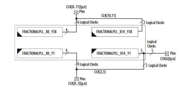