I need a definitive statement regarding the timing.
The two attached screenshots were created with Quartus 23.1 but can also be found in 25.1. Although adjusting the temperature range reduced the number of failing paths (see screenshot 800MHz_300MHz_DDR3_1, which ran at -40°C to 100°C), there remain parts that do not meet the timing.
According to the datasheet, this should work.
The MAX10 being used is a 10M16DAF484I6G, which is the fastest speed grade. The memory is Micron MT41K256M16TW-107AAT.
We will continue to monitor this post for the next 5 days. If there are no further inquiries during this period, I will step back and allow the community to assist with any future follow-up questions.
Unfortunately, the problem has not been resolved even with the references to the manuals on timing. An AI analysis of the failing DDR3 timings states: "This is not a 'real' logic timing error but rather a classic DDR-DQS analysis artifact in the MAX10."
This is justified based on the following three points:
1️⃣ DQS is treated as a normal clock Quartus interprets: "A normal register is clocked by a normal clock (mem_dqs_l_n_OUT)" ❌ This is incorrect for DDR. In reality:
DQS is not a global clock.
DQS is a source-synchronous strobe.
Capture happens in the I/O element, not in the core logic. 👉 Timing between pll_clk → mem_dq → dqs is physically coupled but not logically synchronized.
2️⃣ The clock skew is absurdly high (6.891 ns) This is the second major red flag 🚨:
Clock Skew: 6.891 ns
Setup Relationship: 0.833 ns ➡️ Quartus compares:
PLL clock in the core
Against DQS, which comes from an I/O path. This has no real significance for DDR reads.
3️⃣ PLL compensation appears negative
PLL Compensation: -7.957 ns / -8.063 ns This is typical for:
Generated clocks
DDR IP
DQS paths ➡️ The timing engine is being used outside its optimal range.
Can we use these statements to arrive at a solution?
When switching the FPGA from 10M16DAF484 to 10M08DAF484 in the DDR3 memory controller example design generated from the design, a fitter error occurs
Error (16076): This specific device does not support listening to nsleep port. Parameter "listen_to_nsleep_signal" of atom "ddr3_mem_ctrl_example_if0:if0|ddr3_mem_ctrl_example_if0_p0:p0|ddr3_mem_ctrl_example_if0_p0_memphy_m10:umemphy|ddr3_mem_ctrl_example_if0_p0_dqdqs_pads_m10:dq_ddio[1].ubidir_dq_dqs|altera_gpio_lite:dqs_ddio_io|altgpio_one_bit:gpio_one_bit.i_loop[0].altgpio_bit_i|diff_input_buf.diff_input_buf_with_nsleep.ibuf" must be set to FALSE.
Error (12582): Input port PHYMEMCLOCK of "ddr3_mem_ctrl_example_if0:if0|ddr3_mem_ctrl_example_if0_p0:p0|ddr3_mem_ctrl_example_if0_p0_memphy_m10:umemphy|ddr3_mem_ctrl_example_if0_p0_addr_cmd_pads_m10:uaddr_cmd_pads|addr_cmd_pad_m10:address_gen[0].uaddress_pad|altera_gpio_lite:uadc_pad|altgpio_one_bit:gpio_one_bit.i_loop[0].altgpio_bit_i|out_path_enhanced_ddr.fr_out_data_ddio" must not be connected.
Error (12584): This specific device does not support the enhanced DDR HIO. Parameter "use_enhanced_ddr_hio" of atom "ddr3_mem_ctrl_example_if0:if0|ddr3_mem_ctrl_example_if0_p0:p0|ddr3_mem_ctrl_example_if0_p0_memphy_m10:umemphy|ddr3_mem_ctrl_example_if0_p0_addr_cmd_pads_m10:uaddr_cmd_pads|addr_cmd_pad_m10:address_gen[0].uaddress_pad|altera_gpio_lite:uadc_pad|altgpio_one_bit:gpio_one_bit.i_loop[0].altgpio_bit_i|out_path_enhanced_ddr.fr_out_data_ddio" must be set to FALSE.
Error (171113): The design contains 16 blocks of type "Double data rate I/O input circuitry" but the selected device 10M08DAF484C8G does not support such blocks
If I change the device to 10M16DAF484I6G and run the ddr3_mem_ctrl_example_if0_p0_pin_assignments.tcl, I achieve the same timing values concerning mem_dqs[*]. The timing issue related to clk[4]_afi_clk does not appear in our normal design.
Thus, we also have the same problems in the example design.
For those nsleep error, you need to make sure that the device is 10M16DAF484I6G or support device with DDR3.
Try to add this timing contraint into your sdc file because the reset synchroinzer may cause timing violation set_false_path -from altera_reset_controller:rst_controller*|altera_reset_synchronizer:alt_rst_sync_uq1|altera_reset_synchronizer_int_chain_out -to *:if0|*:p0|*_memphy_m10:umemphy|*_reset_m10:ureset|*_reset_sync:*|reset_reg[*]
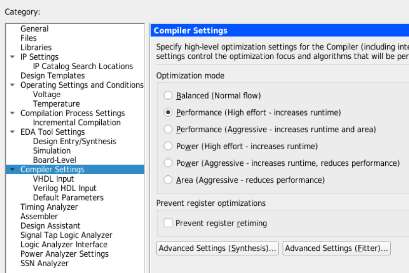
And also set the Compiler setting to Performance:
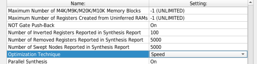
And Optimization Technique to Speed in Advanced Settings (Synthesis):
 New Contributor