Hi,
I have managed to successfully erase and program CFM0 on the 10M04SA device.
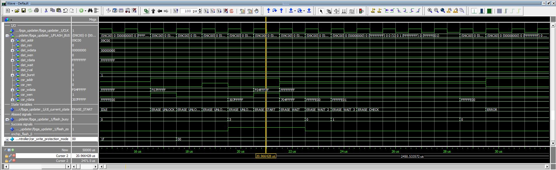
I modified the value written to the flash control register so that all sectors are unlocked. I then send the command to erase sector 4. I updated the file device_pkd.vhd with the code snippet below showing the relevant values.
--! Unlock all sectors & erase sector 4
constant data_flash_unlock :std_logic_vector(31 downto 0) := x"F07FFFFF";
constant data_flash_erase :std_logic_vector(31 downto 0) := x"F04FFFFF";
The erase failed in the same way when the status register transitions from BUSY_ERASE to IDLE early. File "Unlock all sectors 10M04.JPG" shows the flash unlock write and read back from the control register. File "Unlock all sectors erase fail 10M04.JPG" shows the erase failing early.
I then thought I would try this change on the hardware. Again the erase and program failed. However I altered my firmware to stop after the erase so that I could check if the erase had occurred using a Terasic USB Blaster. To my surprise I found that the erase had been successful. I believe this was because my state machine did not go on to program the flash and the erase had time to complete.
After some thought I remembered I had a similar problem with programming on the 10M02. Although the busy field in the status register was retuning to idle the write successful field was never set. For this reason I used only the avmm_data_waitrequest (cfm_dat_wait) to terminate the program cycle.
I wondered if although I was able to use the status register busy and erase successful fields to terminate the erase on the 10M02, maybe they were not working in the same way in the 10M04.
Instead of waiting for the status register busy and erase successful fields I just implemented a timer to wait 400ms. This is comfortably longer than the maximum erase time stated on page 15 of the Intel Max 10 User Flash Memory User Guide, which is 350ms.
Using the timed erase was successful in the hardware and I was able to then reliably program the configuration data into CFM0 of the 10M04SA device. However the simulation was less happy and was giving the following ERROR messages on every write during the programming phase:
tb_fpga_updater.flash_controller.onchip_flash_0.altera_onchip_flash_block.inst.<protected>.<protected>.<protected>.<protected>.<protected>.<protected>: ERROR[0114]: 400127500.00ns, Illegal YADR/ DIN Toggle or 'X' ERROR during prog operation
# tb_fpga_updater.flash_controller.onchip_flash_0.altera_onchip_flash_block.inst.<protected>.<protected>.<protected>.<protected>.<protected>.<protected>.<protected>: ERROR[0196]: 400145206.75ns, An extra program pulse is required for smart-program before regular read cycle
I do not see these messages in the 10M02 simulation. I'm happy the timed erase and program seems to be reliable on the hardware, but it would be nice to have an explanation why the simulation is generating the errors. See files "10M04 Error 0114.JPG" and "10M04 Error 0196.JPG" for the first occurrence of these errors in the simulation.
I removed all the additional states I had added to the state machine and have attached the final working version in file "fpga_updater.vhd". The erase timer is in the attached file "flash_erase_timer.vhd". I added a timer to time out a program operation after 1ms, see file "flash_program_timer.vhd".
 New Contributor