Forum Discussion

Altera_Forum's avatar
Altera_Forum
Icon for Honored Contributor rankHonored Contributor
11 years ago

Help setting Cyclone III pins to 3.3V

Hello,

I am trying to set two pins on the Cyclone III I'm using (EP3C120F780C7N) to work at 3.3V. I'm developing a custom slave I2C controller and the I2C bus will be 3.3V. I changed the pin assignments for this in the pin editor shown below.

https://www.alteraforum.com/forum/attachment.php?attachmentid=9038

When I look at this communication link on the scope I see the microcontroller controlling the data bus at 3.3V when sending, but when the FPGA controls the data bus to send the level is only at 2.5 volts. The bus is pulled up to 3.3V with to 4.7k. The only lines of interest here are really SDA/SCL. When looking at the FPGA talk to the CPU you can see the level difference very clearly. From reading the documentation it seems that pins N26 and R27 should support 3.3V operation.

Any direction/guidance here?
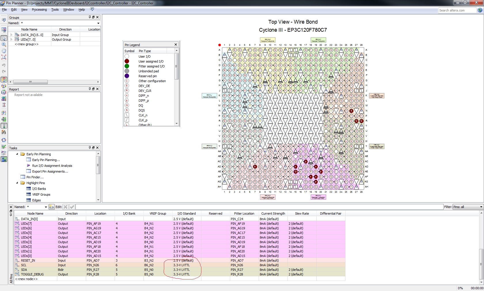
7 Replies

  • Altera_Forum's avatar
    Altera_Forum
    Icon for Honored Contributor rankHonored Contributor

    FPGA pins will not "magically" support an output of 3.3V just by changing the I/O standard to 3.3V :)

    The I/O standard setting in the pin planner has to match the board design, i.e., if you select an I/O standard of "3.3V-LVTTL" then the board also has to have VCCIO = 3.3V in the banks where those pins exist.

    In your case however, because I2C only needs the FPGA to drive low, and you have pull-ups to 3.3V, all you need to do is change your I2C logic. The fact that you can see 2.5V from the FPGA means that you are probably *driving* a logic high from a bank with VCCIO = 2.5V, rather than tri-stating when your I2C controller needs to output a logic high. The pins in the 2.5V bank will tolerate the 3.3V pull-up voltage.

    Cheers,

    Dave
  • Altera_Forum's avatar
    Altera_Forum
    Icon for Honored Contributor rankHonored Contributor

    Hey Dave,

    Thanks so much for the reply. So I'm using the Altera Cyclone II development board from Altera. It sounds like the board is designed such that the bank of pins I'm using are powered as you said by 2.5V. So I can just use high impedance output 'Z' when I want a high and it will allow the bus to be pulled up to 3.3v?
  • Altera_Forum's avatar
    Altera_Forum
    Icon for Honored Contributor rankHonored Contributor

    --- Quote Start ---

    So I'm using the Altera Cyclone II development board from Altera. It sounds like the board is designed such that the bank of pins I'm using are powered as you said by 2.5V.

    --- Quote End ---

    There is no need to guess. Install the development kit software and review the schematic. Tell me what the kit is, and I'll point you to the correct page in the schematic.

    --- Quote Start ---

    So I can just use high impedance output 'Z' when I want a high and it will allow the bus to be pulled up to 3.3v?

    --- Quote End ---

    If you are implementing I2C, then you *should* be tri-stating to implement a logic high. Why? Well, some I2C devices can clock-stretch by driving the I2C clock signal low. If you have one of those devices and your FPGA drives high, then you will have a buffer conflict, and could possibly damage your FPGA or device SCL buffers.

    Cheers,

    Dave
  • Altera_Forum's avatar
    Altera_Forum
    Icon for Honored Contributor rankHonored Contributor

    ok well that makes sense. I've attached the schematics for my board. Could you point me to the place in here where the bank voltage for the banks I'm using for the pins above is listed? I don't see the VCCIO setting for pins for N26 and R27.

  • Altera_Forum's avatar
    Altera_Forum
    Icon for Honored Contributor rankHonored Contributor

    --- Quote Start ---

    I've attached the schematics for my board. Could you point me to the place in here where the bank voltage for the banks I'm using for the pins above is listed? I don't see the VCCIO setting for pins for N26 and R27.

    --- Quote End ---

    Look at the second page of the schematic. This is a screen-capture of the Quartus Pin Planner. If you open the Pin Planner in Quartus you'll be able to find N26 and R27 and see what their bank number is a bit easier than in this screen capture, since its blurry. However, you can see that N26 is Bank 6, which has a VCCIO = 2.5V, and R27 is Bank 5, which also has VCCIO = 2.5V.

    Now, page 2 is only what the designer "says" the VCCIO is supposed to be, we can look further through the schematic to confirm this.

    Go to the power supply design on p6 and you can then see that VCCIO5 and VCCIO6 connect to 2.5V_B5_B6, which shows that these two banks connect to a common 2.5V power source. Page 4 shows how that 2.5V is generated via an LT1963A linear regulator.

    Cheers,

    Dave
  • Altera_Forum's avatar
    Altera_Forum
    Icon for Honored Contributor rankHonored Contributor

    Dave thanks so much! That makes sense so I'm good now. I'll change over to setting the bust to 'Z' when I have a 1 to send over the I2C bus from the slave. This was a great help and really cleared this up for me!

    Thanks,

    Rob
  • Altera_Forum's avatar
    Altera_Forum
    Icon for Honored Contributor rankHonored Contributor

    --- Quote Start ---

    That makes sense so I'm good now.

    --- Quote End ---

    Great!

    --- Quote Start ---

    I'll change over to setting the bust to 'Z' when I have a 1 to send over the I2C bus from the slave. This was a great help and really cleared this up for me!

    --- Quote End ---

    You can easily make the change at the top-level of your design. Lets say your outputs are scl_out and sda_out, then the tri-state/low drivers in VHDL are;

    
    scl <= 'Z' when (scl_out = '1') else '0';
    sda <= 'Z' when (sda_out = '1') else '0';
    

    Cheers,

    Dave