Altera_Forum Honored Contributor
Honored ContributorHonored ContributorHonored ContributorFPGA pins will not "magically" support an output of 3.3V just by changing the I/O standard to 3.3V :)
The I/O standard setting in the pin planner has to match the board design, i.e., if you select an I/O standard of "3.3V-LVTTL" then the board also has to have VCCIO = 3.3V in the banks where those pins exist. In your case however, because I2C only needs the FPGA to drive low, and you have pull-ups to 3.3V, all you need to do is change your I2C logic. The fact that you can see 2.5V from the FPGA means that you are probably *driving* a logic high from a bank with VCCIO = 2.5V, rather than tri-stating when your I2C controller needs to output a logic high. The pins in the 2.5V bank will tolerate the 3.3V pull-up voltage. Cheers, Dave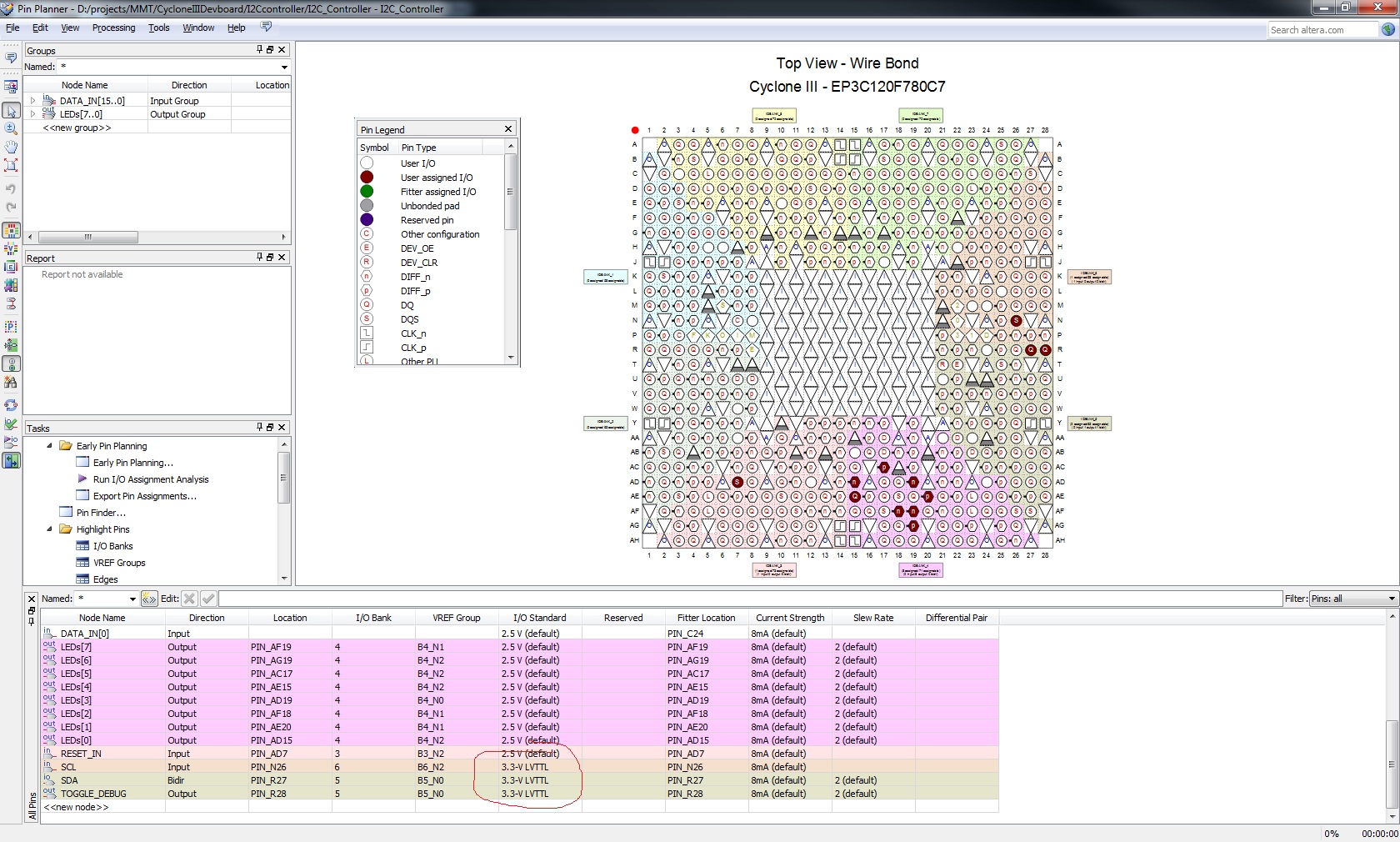