--- Quote Start ---
I've attached the schematics for my board. Could you point me to the place in here where the bank voltage for the banks I'm using for the pins above is listed? I don't see the VCCIO setting for pins for N26 and R27.
--- Quote End ---
Look at the second page of the schematic. This is a screen-capture of the Quartus Pin Planner. If you open the Pin Planner in Quartus you'll be able to find N26 and R27 and see what their bank number is a bit easier than in this screen capture, since its blurry. However, you can see that N26 is Bank 6, which has a VCCIO = 2.5V, and R27 is Bank 5, which also has VCCIO = 2.5V.
Now, page 2 is only what the designer "says" the VCCIO is supposed to be, we can look further through the schematic to confirm this.
Go to the power supply design on p6 and you can then see that VCCIO5 and VCCIO6 connect to 2.5V_B5_B6, which shows that these two banks connect to a common 2.5V power source. Page 4 shows how that 2.5V is generated via an LT1963A linear regulator.
Cheers,
Dave
 Honored Contributor
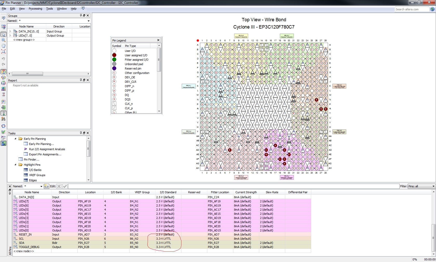