Altera_Forum Honored Contributor
16 years agoHonored ContributorFilter & decimation implementation on AD7401
Hello everybody!
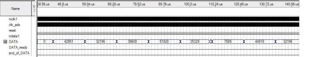
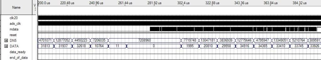
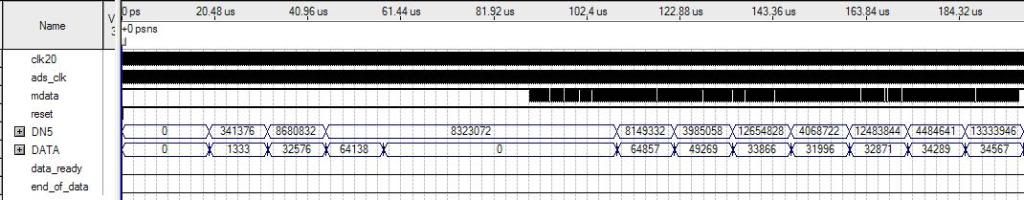
We have chosen the AD7401 Sigma Delta modulator for our project, translated the Verilog code given by the datasheet into VHDL and are now confused about the results of the simulation. We have attached our translated VHDL code plus the datasheet of AD7401. 1) We will give the master clock from the FPGA to the ADC from one of the I/O pins. The clocks don't seem to be synchronized though, there is a 5nsec latch delay. Should that be ok, or do we have to eliminate that delay somehow? 2) We tried to simulate the data flow inputting only ones '1', but result is really not the expected one. (DATA samples should be at the highest level?!) Yes, but what about overflow? The given interface is permitting that, if such a case comes up. Below are some results of a random inputted bit stream and a only '1' bit stream. http://i252.photobucket.com/albums/hh3/unoturbomk2/samples.jpg http://i252.photobucket.com/albums/hh3/unoturbomk2/samples2.jpg *** Is the code correct? *** We'd appreciate any kind of help! Thanks in advance!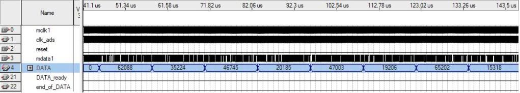