Hi Sstrell,
I thought I’d successfully replied several days ago, but apparently it didn’t take. My responses embedded below in red.
Thanks,
Bill
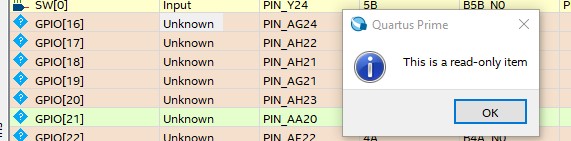
You can't use the same name for multiple top-level ports, as the error states. Yes, completely understand. You could have something like GPIO_in and GPIO_out, each with the appropriate range, [15:0] and [19:0], respectively. This is where I’m having trouble. I tried very similar pin naming, but, because they’re not named exactly GPIO, Quartus assigns them other than GPIO Pins. I tried using Pin Planner to reassign them to GPIO Pins. But, because they’re reserved for GPIO I guess, I’m told they already in use. The pinout of the device, configured in the Pin Planner, is where you'd differentiate between the upper 20 pins and the lower 16. I suspect this is the answer, but I haven’t been able to figure out how to do. Would you please elaborate?
Same thing for your schematic. And there's nothing wrong with a top-level HDL file. But to add the schematics, you have to instantiate them in the HDL code like any other code instantiation:
<component name> #(<parameter mapping if any>) <instance name> (<port map>);
For example for a simple multiplier with a single parameter, give it a unique instance name, pass in the mult_size value to the width_in parameter, and map each signal in top-level HDL code with the port in the instantiated design:
multa #(.width_in(mult_size))
u1 (.in_a(dataa), .in_b(datab), .mult_out(mult_out));
The dot (.) ports are the ports of the lower-level design. The signal names in parentheses are the signals they connect to.
If you're not familiar with the basics of Verilog, this is a good place to start:
https://learning.intel.com/developer/learn/course/external/view/elearning/235/verilog-hdl-basics Thanks, I’ll definitely study. I’ve come to appreciate how powerful HDL is compared to conventional schematics. However, for this project, I need the schematic, visual presentation.
 Occasional Contributor
