BillM256 Occasional Contributor
Occasional ContributorOccasional ContributorCase closed! Many thanks!
Occasional ContributorHi Sstrell,
I thought I’d successfully replied several days ago, but apparently it didn’t take. My responses embedded below in red.
Thanks,
Bill
You can't use the same name for multiple top-level ports, as the error states. Yes, completely understand. You could have something like GPIO_in and GPIO_out, each with the appropriate range, [15:0] and [19:0], respectively. This is where I’m having trouble. I tried very similar pin naming, but, because they’re not named exactly GPIO, Quartus assigns them other than GPIO Pins. I tried using Pin Planner to reassign them to GPIO Pins. But, because they’re reserved for GPIO I guess, I’m told they already in use. The pinout of the device, configured in the Pin Planner, is where you'd differentiate between the upper 20 pins and the lower 16. I suspect this is the answer, but I haven’t been able to figure out how to do. Would you please elaborate?
Same thing for your schematic. And there's nothing wrong with a top-level HDL file. But to add the schematics, you have to instantiate them in the HDL code like any other code instantiation:
<component name> #(<parameter mapping if any>) <instance name> (<port map>);
For example for a simple multiplier with a single parameter, give it a unique instance name, pass in the mult_size value to the width_in parameter, and map each signal in top-level HDL code with the port in the instantiated design:
multa #(.width_in(mult_size))
u1 (.in_a(dataa), .in_b(datab), .mult_out(mult_out));
The dot (.) ports are the ports of the lower-level design. The signal names in parentheses are the signals they connect to.
If you're not familiar with the basics of Verilog, this is a good place to start:
https://learning.intel.com/developer/learn/course/external/view/elearning/235/verilog-hdl-basics Thanks, I’ll definitely study. I’ve come to appreciate how powerful HDL is compared to conventional schematics. However, for this project, I need the schematic, visual presentation.
 Regular Contributor
Hello,
I just noticed that this case has just been re-opened. Since your last post has been awhile ago may I know which specific problem are you facing?
Thank you.
Regular ContributorHello Bill,
Is there any update from you?
Thank you.
Occasional ContributorHi Amin,
I understand from Ashlesha that you've agreed to help, many thanks!
I never closed this case; I just didn't get an answer to my last post.
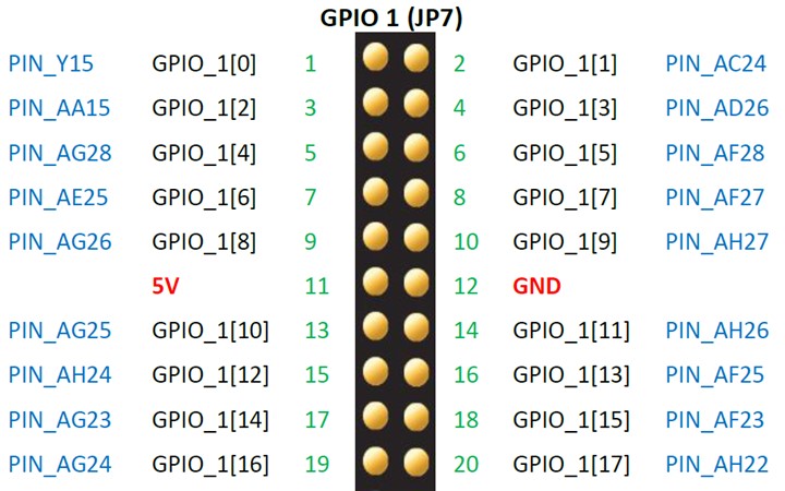
The open issue is mixing inputs and outputs on a single GPIO header of a DE10-Nano. Simple example: GPIO_1[1] = Input; GPIO_1[2] = Output; (and perhaps GPIO_1[3] = BiDir). My original post gives more detail including things I tried unsuccessfully.
Seems this should be easy, but I haven't figured it out, and, so far, no one has furnished the explanation.
Thanks again,
Bill
 Super Contributor
I never saw this response so never responded. The names you give have absolutely no affect on their use. Naming something "GPIO" doesn't mean anything to the compiler other than you have a top-level I/O named "GPIO". I'm not sure I understand what issue you are seeing. You say "I'm told they already in use." What does this mean? What error are you seeing? Can you post screenshots or better describe what is not working as you expect?
If you do not create specific pin location assignments in the Pin Planner, the Fitter creates suggested assignments that would be used if you programmed the device. You use the Pin Planner to pick the specific locations you want to use.
Occasional ContributorHi Sstrell,
Thanks for the info. As before, I've embedded my specific responses in red.
I've also included several attachments:
1. Schematic portion
2. Pin Planner auto-assignments
3. GPIO_1 pins
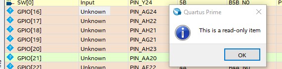
4. Error when I try to manually assign GPIO_1[16]
I never saw this response so never responded. Not surprised; my initial reply was dropped and I had to repost several days later. The names you give have absolutely no affect on their use. Naming something "GPIO" doesn't mean anything to the compiler other than you have a top-level I/O named "GPIO". My experience is different. If I only spec GPIO_1 input pins in the .V, I get a clean compile and Pin Planner is updated with those pins in the process. See attachments 2 and 3. I'm not sure I understand what issue you are seeing. You say "I'm told they already in use." What does this mean? What error are you seeing? As described, the GPIO_1 input pins were assigned automatically for me (Fitter?) Now my problem is to assign my GPIO_1 output pins, starting with [16], which is PIN_AG24. This is where I get the error shown in attachment 4. Can you post screenshots or better describe what is not working as you expect?
If you do not create specific pin location assignments in the Pin Planner, the Fitter creates suggested assignments that would be used if you programmed the device. You use the Pin Planner to pick the specific locations you want to use.
Thanks as always,
Bill