Altera_Forum Honored Contributor
Honored ContributorHonored ContributorHi, this is a simple counter with asynch pre-set(not wired in diagram), enable, load and synch add +1. i can't figure the trick to get rid of one extra mux column and use the FF enable (where red arrow is). Do you have any ideas please?
cheers. Pretty sure there's a way to do it....Honored Contributorthe way you guys describe solutions is kinda how you want to synthesizer to design the logic for your needs. I think that's very power full and is gained after years of experience. This one for example :
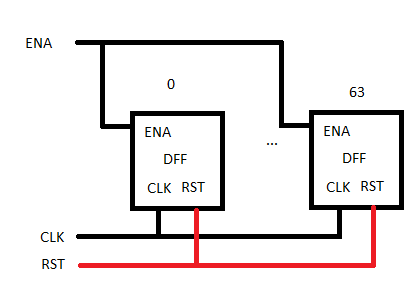
--- Quote Start --- load enable cnt 0 0 no change of cnt 0 1 count up, may not get initialised 1 0 load value to cnt 1 1 count up --- Quote End --- Would you kindly explain this methodology please Kaz? As in how you picture the logic will be for the code you describe and the other way round, how do you describe code to get these states (if it makes sense) ? Also one more thing, in the picture I attached the Load input is driving multiple multiplexers. Is there a trick behind the scenes that takes care of the driving capabilities inside the FPGA. As in can one input drive all that logic at one internally? (is my question clear here?)Honored ContributorHonored ContributorSo lets say we have 64 DFFs (as in picture attached) each requiring a clk, rst and enable in parallel. I guess that's quite a lot of driving current needed right?
1. how do i measure the actual driving current needed? 2. is it good practice to connect all 64 (clk, rst and ena) together in parallel like in the picture, and drive them from just one input? 3. say clk is driven internally from a PLL, can the PLL drive all those FF? can it supply enough current to all? Or is there a limit some where in a datasheet? 4. say rst is driven from an external pin, can this pin handle the current needed? 5. transient currents create a lot of noise... 6. are there any fanout techniques used internally in the FPGA to split signals, like clk, rst and ena, in this case, to say groups of 8?Honored ContributorHonored ContributorAssuming you have connected the FPGA to the board as per the instructions in the data sheet with the correct Vcc and Ground Pins, then current draw wont be a worry as it will always be within the spec on the datasheet.
There is a power analysis tool that can run your design through to give estimated power draw for your design, but that may be a bit advanced for what you are doing. Just be assured that if the design fits in the device and meets timing (and you have designed it to correct correctly with the connected IOs) then it will work.Honored Contributorthanks for the observations. Quite advanced yes. Was just thinking about it so i asked.
Honored Contributor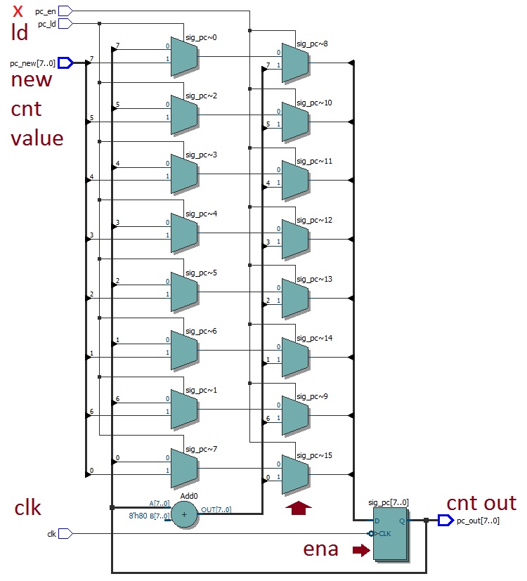