Forum Discussion

Altera_Forum's avatar
Altera_Forum
Icon for Honored Contributor rankHonored Contributor
7 years ago

SPI Slave Timing Constraint Question

Hi,

I have designed an spi slave component and am having problems working out the best/correct way of creating timing constraints for the interface.

A quick description of my component: The input nss sclk and mosi signals are sunk to an internal clk domain running faster than the max spi clock freq. I am evaluating the nss and sclk edges and shift in data from the mosi signal and shift data back out on the miso signal. (see attached diagram)

I am not sure how to constrain this interface to pass timing. As I am syncronising the incoming signals to an internal clock via 2 registers I was thinking I should false path from the input pins to the internal register stage as they are crossing clock domains.

At the same time I am concerned that the relationship between sclk and mosi/miso is important and I want the fitter to know to to place the registers in a way that maintains the relationship. I am also unsure how to describe the relationship required for my miso output signal which needs to maintain a setup/hold relationship to sclk.

Here is roughly what I am thinking (note these are not correct sdcs):

describe the incoming spi signal relationships:


create_clock -name {virtual_sclk} -period $period_sclk
set_input_delay -clock virtual_sclk -max $maxdelays 
set_input_delay -clock virtual_sclk -min $mindelays 

then false path the input port to register? or would this be a time to use set_max_delay?

//false path option
set_false_path -from  to 
// or max delay
set_max_delay -from  to  $somedelay

I was thinking for the miso I could set output min/max delay wrt virtual_sclk?

set_output_delay -clock {virtual_sclk} -max/min $max/mindelays 
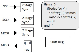
but miso is being generated at my internal clock domain and I cant sync it back to the virtual_sclk domain so I guess the timing analysis wouldnt be valid and end up with a setup relationship of the closest the two edges could get?

Any help or advice would be appreciated.

Thanks

James

5 Replies

  • Altera_Forum's avatar
    Altera_Forum
    Icon for Honored Contributor rankHonored Contributor

    Hi James,

    Why are you not using the sclk to clock your data ?

    This clock is synchronous with your other signals and you will not have to add the double registers.

    In this case, your constraint file will be very simple.

    Jerome
  • Altera_Forum's avatar
    Altera_Forum
    Icon for Honored Contributor rankHonored Contributor

    Hmm thats a good question. When starting out I thought this method seemed to better fit with the data flow control I have surrounding the slave component. It also required less asynchronous design and less handshaking with the internal clock domain. When nss and sclk are idle I would be using control signals to update buffers etc. rather than clocking them per normal synchronous design. On the upside it would increase the max spi freq the component could support.

    I am putting together another slave component with the spi sclk directly controlling the shifting as per your suggestion. But for the sake of argument would the timing constraints I have suggested constrain the original design?

    James
  • Altera_Forum's avatar
    Altera_Forum
    Icon for Honored Contributor rankHonored Contributor

    Actually an SPI slave where all the inputs are synchronised with a double register-chain doesn't need to be constrained. The

    set_false_path -from  -to *
    will do. As the miso is clocked by a higher frequency clock a
    set_false_path _from * -to miso
    is OK too.

    The same reasoning applies for the case of an SPI Master (reversing the directions of the false paths)
  • Altera_Forum's avatar
    Altera_Forum
    Icon for Honored Contributor rankHonored Contributor

    --- Quote Start ---

    I am putting together another slave component with the spi sclk directly controlling the shifting as per your suggestion. But for the sake of argument would the timing constraints I have suggested constrain the original design?

    James

    --- Quote End ---

    IMO the so-called SPI clock isn't a real clock as it isn't continuous. The original author should have called it Strobe.
  • Altera_Forum's avatar
    Altera_Forum
    Icon for Honored Contributor rankHonored Contributor

    --- Quote Start ---

    Actually an SPI slave where all the inputs are synchronised with a double register-chain doesn't need to be constrained.

    --- Quote End ---

    My concern is that be cutting all the spi paths you cant guarantee the fitter is going to place the registers in a repeatable way. I believe as long as the internal clk is a lot faster than the spi clock like 10x, its not going to be a problem but as the freq increases you might get one fit work and one fit not work.

    --- Quote Start ---

    IMO the so-called SPI clock isn't a real clock as it isn't continuous. The original author should have called it Strobe.

    --- Quote End ---

    Yes from the FPGAs internal point of view its not a true clock but from the spi data point of view it is a clock. IMO I would prefer the hdl signals to match the standard interface signal names but in the end the naming is negligible.