Forum Discussion

 New Contributor
Global Clock & Regional clock inputs in Agilex M FPGA
 New Contributor
Hi,
Please find the attached diagram based on Agilex M FPGA.
We want to know the function of USB interface in this board. Any document giving the details would be great.

 Regular Contributor
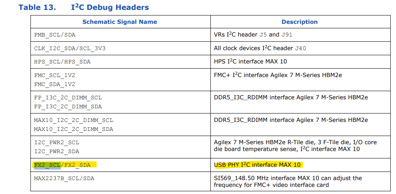
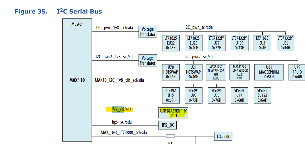
This is what I found in the Agilex 7 FPGA M-Series HBM2e Development Kit User Guide on the description of the signal connecting to this USB PHY.
Regards,
- Thulasi2 months ago
Hi,
Thanks a lot for the reply. But, why do we need USB PHY in Agilex M FPGA based board. To program, MAX10/Agilex, JTAG interface will provide. But,what extra functionality that USB Interface provides in the board ?
Regards,
Thulasi
- AqidAyman_Altera1 month ago
Hi Thulasi,
After checking the connection, we determine that is USB to JTAG which it is for the on-board USB blaster II.
Regards,
Aqid- Thulasi1 month ago
Hi,
1. Why do we need to provide both a JTAG header and a USB connector (along with its supporting circuitry) for JTAG access?
2. Can we eliminate the USB circuitry and provide only the JTAG header?
3. Alternatively, can we remove the JTAG header and retain only the USB connector and its associated circuitry?
4. Why is an on-board USB-Blaster II required? Wouldn't a standard JTAG header alone be sufficient for programming and debugging?
Regards,
Thulasi


