Forum Discussion

bwa555221's avatar
bwa555221
Icon for New Contributor rankNew Contributor
2 years ago
Solved

Internal Error when attempting to program Agilex 7 on Intel Development Kit

Unabel to program Agilex 7 development kit, DK-DEV-AGF014EA, which uses AGFB014R24B2E2V

A standalone (HPS only) design successfully compiled in Quartus Prime Pro 23.3.0.104 (latest release). Unable to program .sof to FPGA. Design is in FPGA-first boot mode.

hps_auto_<project_name>.sof is generated via quartus_pfg tool with the following command:

quartus_pfg -c -o compression=ON -o hps_path=%spl_dir% "%sof_dir%" "%rbf_dir%"

Where the variable “spl_dir” points to the u-boot-spl-dtb.hex file that is rolled into the .sof.

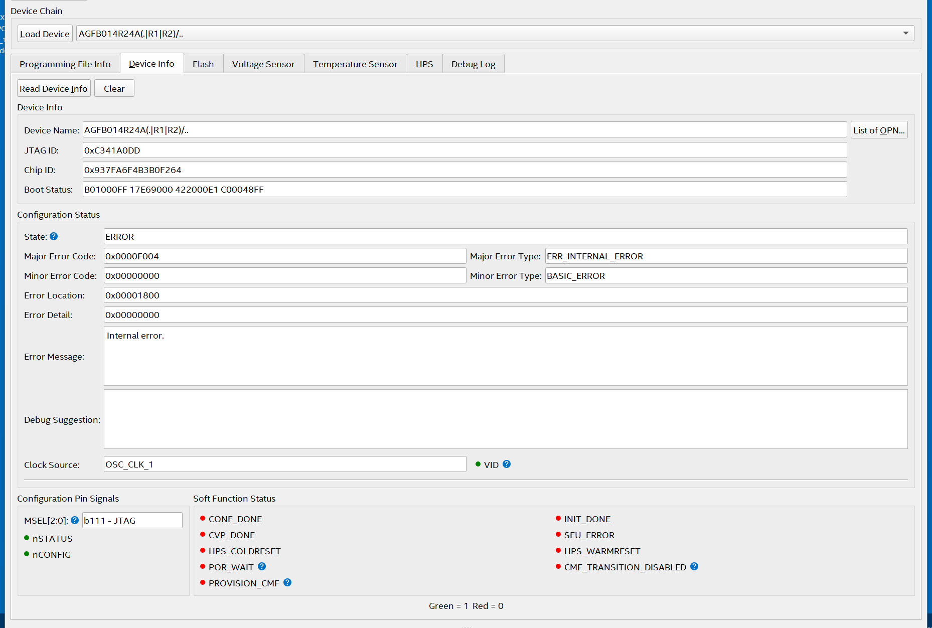
When attempting to flash FPGA via JTAG I received the following error about ~50% into the programming process.

Receiving error “Device has stopped receiving configuration data” through “Internal Error” with Major Error Code: 0XF004, which indicates “Indicates an internal error due to misunderstood bitstream element”, per this resource:

https://www.intel.com/content/www/us/en/docs/programmable/683290/22-4-20-2-1/appendix-config-status-and-rsu-status.html

All SDM configuration and pin maps are pulled from GHRD for this development kit. I have manually stepped through the Configuration Debugging Checklist located here:

https://www.intel.com/content/www/us/en/docs/programmable/683673/23-3/configuration-debugging-checklist.html

I have manually checked MSEL pins, all other DIP switches, and confirmed presence and stability of reference clock signals with an oscilloscope.

I am attaching a .7z of my design (just a single VHDL top level file and the QSYS block with the HPS in it). I also have attached the analysis of my .sof file and a status capture of the SDM, as performed by the Configuration Debugging Utility.

Can someone please review my design, or point me a direction to troubleshoot? The error message is non-descript and does not help much at all.

Thanks!

  • Hi Jingyang,

    Thank you very much for your help with this. The data points you have provided have helped greatly in debugging and verification of programming procedure.

    This case has transitioned over to IPS support. I/We can close this ticket and accept solution.

    Thanks,

    Brandon

8 Replies

  • tehjingy_Altera's avatar
    tehjingy_Altera
    Icon for Regular Contributor rankRegular Contributor

    Hi

    I am Jingyang and was assigned to this case.

    Please give me sometime to take a look at the case and reply you as soon as possible.

    Regards

    Jingyang, Teh

  • tehjingy_Altera's avatar
    tehjingy_Altera
    Icon for Regular Contributor rankRegular Contributor

    Hi

    I just tried out the design that you created.

    There is a sof file "pcie_test_hps_auto.sof", I assume it is the final sof that you created with the bootloader combined.

    Tried it out on the devkit on my end and the flashing completed successfully.

    There are logs from the devkit too, however there are some problem with the ddr calibration. Refer below:

    Before we deep dive into your design, lets confirm that the board you are having is working properly.

    Have you tried successfully booting the board you have?

    If not there are steps on running our GSRD first. Do take note to follow the steps for the DK-SI-AGF014EA.

    https://www.rocketboards.org/foswiki/Documentation/AgilexSoCGSRD

    Regards

    Jingyang, Teh

  • bwa555221's avatar
    bwa555221
    Icon for New Contributor rankNew Contributor

    Hi Jingyang,

    Thank you for providing this valuable data point.

    As for the SDRAM calibration, I disabled the EMIF calibration from with Platform Designer, so I understand why this fails.

    I am not so concerned with being unable to boot Linux, since I am not even able to complete the flashing of the bitstream like you were able to do.

    I do have another test design, which does not use the HPS, only a standalone P-tile PCIe MCDMA IP, and that design compiles, programs, and works just fine (reading the VID/PID of the PCIe IP on the DK from a host Linux machine over the PCIe interface). So I think my board is "working" just not when I include the HPS system.

    At the point I am fairly convinced there is an issue with my DK, since I have already verified all clocks and voltages are present and stable, and you have been able to successfully verify my design and bitstream.

    Before I work through an RMA of this unit, are there perhaps any other suggestions you may have?

    I tried slowing JTAG programming speed down to 6 MHz from 24 MHz and this did not show any improvement. Same results with USB-Blaster JTAG and on-board USB JTAG programmer also.

    Thanks for your time,

    Brandon

    • bwa555221's avatar
      bwa555221
      Icon for New Contributor rankNew Contributor

      Hi Jingyang,

      Thank you for your feedback.

      I have not had a chance to try the GSRD yet. I am willing to give the GSRD an attempt if that is what you advise. However, I am in the U.S., working remotely the first part of the week and we have holiday events later this week. I likely won't be able to provide a further update until I am back in the office and able to test the GSRD - I expect this to be 11/27.

      I have also contacted my Intel account technical representative who is working on getting an IPS ticket setup for this issue. He is aware we have been working this issue, you may be contacted internally.

      Regards,

      Brandon

      P.S. - For completeness, attaching the DIP switch settings being used on my board:

      DIP switch settings for PCIe P-tile DK:

      Legend:
      O => OPEN
      C => CLOSED
      x => DON'T CARE

      ######### STANDALONE CONIFGURATION ###########
      SW1 (MSEL)
      OOOx : JTAG programming mode only


      SW2
      OOOO : USB JTAG Enabled, Si5341 enabled, PCIe on-board ref clock enabled, UART enabled


      SW3
      OOOO : Enable all PMBUS and I2C slaves


      SW4 (JTAG chain selects)
      OOCO : UBII JTAG enabled (no PCIe JTAG), Bypass MICTOR JTAG (HPS), ENABLE FPGA, ENABLE MAX10 in JTAG CHAIN


      SW5 (Power switch)
      x : ON/OFF


      SW6 (PCIe configuration)
      COOO : Set for PCIe x16 mode


      SW7
      C : Select PCIe ref clock from Si clock IC
      ##############################################

  • tehjingy_Altera's avatar
    tehjingy_Altera
    Icon for Regular Contributor rankRegular Contributor

    Hi Brandon


    Any update on this case?

    Have you managed to test out the GSRD on your dev kit?


    Regards

    Jingyang, Teh


  • tehjingy_Altera's avatar
    tehjingy_Altera
    Icon for Regular Contributor rankRegular Contributor

    Hi


    Since there are no feedback for this thread, I shall set this thread to close pending. Please login to ‘https://supporttickets.intel.com’, view details of the desire request, and post a feed/response within the next 15 days to allow me to continue to support you. After 15 days, this thread will be transitioned to community support. The community users will be able to help you on your follow-up questions.


    If you happened to close this thread you might receive a survey. If you think you would rank your support experience less than 10 out of 10, please allow me to correct it before closing or if the problem can’t be corrected, please let me know the cause so that I may improve your future service experience.


    Regards

    Jingyang, Teh


  • bwa555221's avatar
    bwa555221
    Icon for New Contributor rankNew Contributor

    Hi Jingyang,

    Thank you very much for your help with this. The data points you have provided have helped greatly in debugging and verification of programming procedure.

    This case has transitioned over to IPS support. I/We can close this ticket and accept solution.

    Thanks,

    Brandon