 New Contributor
Clocking Network (Quartus prime pro 20.2)
Hi,
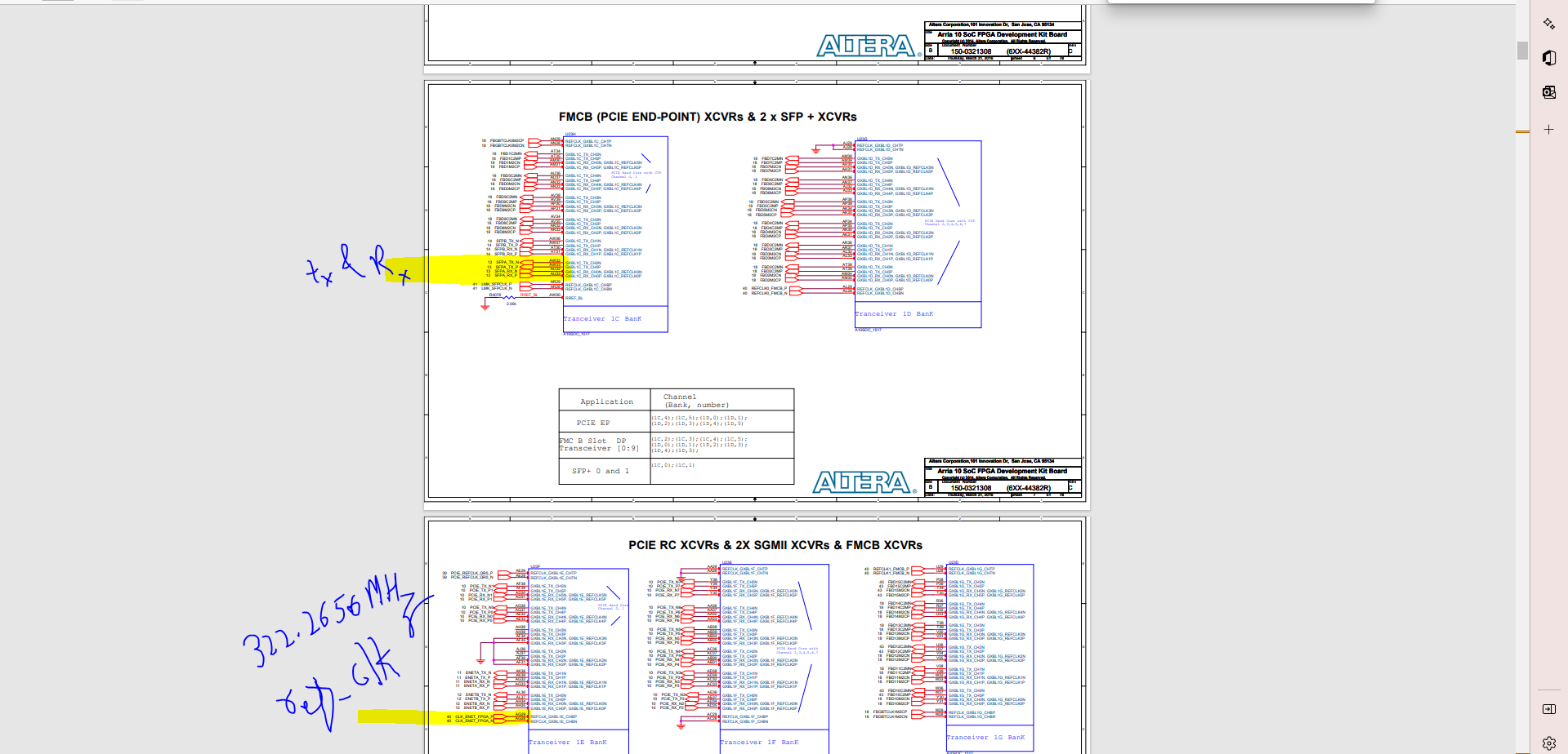
I generated low latency MAC example design from the Quartus prime pro 20.2(screenshot attached for reference - 10G_base_R_design_example.png) ; in the ATX pll IP for PHY, I did not choose any option related to MCGB, bonding or xN clocking (screenshot attached for reference - MCGB_default_reference.png) . But I assigned the clock from 1E bank (PIN_AG29) directly as reference clock for my SFP transceiver (present in 1C bank - PIN_AW33 for tx and PIN_AU33 for Rx).
Generating the build was successful. Even though I am taking reference clock from some other bank without even enabling xN clocking or bonding or MCGB, I did not get any error. I am confused how is it happening. Is this version of Quartus routes to clock intelligently (inter bank clocking).
Kindly help I am confused. My device and design details are as follows -
Development kit - Arria 10 SX SOC development kit (https://www.intel.in/content/www/in/en/products/details/fpga/development-kits/arria/10-sx.html)
Board - 10AS066N3F40E2SG
Schematic diagram referred - Arria 10 SOC revC (a10_soc_devkit_03_31_2016.pdf)
Kindly let me know if more info required from my side.
Thank you
Regards
Shubhangi
