memory controllers
278 Topics
Why does the dynamic reconfiguration simulation of Phylite IP design fail in the Questa* – Altera® FPGA Edition ?
Description Due to a problem in the External Memory Interfaces (EMIF) IP, simulation running in the Questa* – Altera® FPGA Edition might fail when you set the use dynamic reconfiguration on Agilex® 7M R0 devices. Resolution To work around this problem, change the device selection to a non-R0 OPN during simulation.6Views0likes0CommentsWhy does the High Bandwidth Memory (HBM2E) Interface Agilex® 7 IP fail generation after disabling Reserve Channel 2 and Channel 3 for HPS boot from HBM?
Description Due to a problem in the Quartus® Prime Pro Edition Software version 26.1.1, the High Bandwidth Memory (HBM2E) Interface Agilex® 7 IP Interface IP GUI does not correctly handle the "Reserve Channel 2 and Channel 3 for HPS boot from HBM" option when it is disabled after being enabled. After enabling the option and subsequently unchecking it, the IP may enter an inconsistent configuration state and fail during IP generation. Users may observe interface mismatch errors similar to the following: Error: hbm2e.hbm_fp_0: Interface t_ch2_u0_axi4noc is not the same type as exported interface tniu_ch2_u0.target_inst_0 (should be a hps_axi4noc) Error: hbm2e.hbm_fp_0: Interface t_ch2_u1_axi4noc is not the same type as exported interface tniu_ch2_u1.target_inst_0 (should be a hps_axi4noc) Error: hbm2e.hbm_fp_0: Interface t_ch3_u0_axi4noc is not the same type as exported interface tniu_ch3_u0.target_inst_0 (should be a hps_axi4noc) Error: hbm2e.hbm_fp_0: Interface t_ch3_u1_axi4noc is not the same type as exported interface tniu_ch3_u1.target_inst_0 (should be a hps_axi4noc) Error: hbm2e.hbm_fp_0: Interface t_ch2_ch3_sb_axi4noc tried to export unknown interface tniu_ch2_ch3_sb.target_inst_0 The issue is only observed after toggling the HPS boot from HBM option from enabled to disabled. Resolution As a workaround, if the "Reserve Channel 2 and Channel 3 for HPS boot from HBM" option is enabled by mistake, close and restart the IP Parameter Editor GUI without saving any changes. Reopen the IP and continue the configuration with the desired setting. This problem is scheduled to be resolved in a future release of the Quartus® Prime Pro Edition Software.150Views0likes0CommentsWhy do I see RRESP=2 if ECC is enabled in External Memory Interfaces (EMIF) IP?
Description When ECC is enabled in External Memory Interfaces (EMIF) IP of Agilex® 7 FPGA M-Series, Agilex® 5 FPGA, and Agilex® 3 FPGA devices, you might receive RRESP=2 during data readback if any of the following conditions is true. DDR4 Component: Data size of the first write command to the associated AXI4 address ≠ 256 bits * N DDR5 Component/DDR5 DIMM/LPDDR4/LPDDR5: Data size of the first write command to the associated AXI4 address ≠ (Channel DQ width * 16) * N where N is a positive integer (1, 2, 3, ...). The hard memory controller uses fixed DQ burst length. The above conditions generate partial access to the memory. The uninitialized portion of data in the memory will cause uncorrectable ECC error, leading to RRESP=2. Below are some example scenarios that showcase this RRESP problem. Example #1: When using a x16+ECC DDR4 Component interface in fabric accessing mode, the first write command to an AXI4 address is a partial access with the use of WSTRB. WDATA width = 256 bits, AWLEN = 0, WSTRB = 0x0000FFFF: Data size of the first write command to the associated AXI4 address = 128 bits Example #2: When using a 1chx32 LPDDR5 interface with in-line ECC enabled in fabric accessing mode, the first write command to an AXI4 address has only one WDATA beat. WDATA width = 256 bits, AWLEN = 0: Data size of the first write command to the associated AXI4 address = 256 bits Channel DQ width * 16 = 512 bits Example #3: When using a x32+ECC DDR5 RDIMM interface in 256-bit NoC accessing mode, the first write command to an AXI4 address uses an even number AWLEN value. WDATA width = 256 bits, AWLEN = 2: Data size of the first write command to the associated AXI4 address = 768 bits Channel DQ width * 16 = 512 bits Resolution To work around this problem, ensure the data size of the first write command to the associated AXI4 address equals to either 256 bits * N or (Channel DQ width * 16) * N, depending on the memory protocol. An alternative method is available starting with Quartus® Prime Pro Edition Software version 26.1.1. When IP parameter Initialize Memory in the Advanced Calibration Settings section is enabled, on calibration passing, and before handing off control of the memory to user logic, the memory will be initialized with all zeros in the data section and the corresponding ECC codes in the ECC section. With this approach, there is no special requirement on the data size of the first write command to the associated AXI4 address. Note: To avoid leading to long simulation time, only the first 256 bytes of memory will be initialized in simulation when Initialize Memory is enabled. Additional Information DDR4 DIMM interface and LPDDR5 interface using link ECC are not affected by this RRESP problem.56Views0likes0CommentsWhy does U-Boot initially read incorrect information from the EMIF controller Read-Only registers, but later retrieve the correct information on Agilex® 3, Agilex® 5, and Agilex® 7 FPGA M-Series devices in Quartus® Prime Pro edition software 26.1.1 and earlier?
Description Due to a synchronization issue between U-Boot and the IOSSM firmware, U-Boot may read incorrect values from EMIF controller read-only registers, such as MAILBOX_HEADER and MEM_TOTAL_CAPACITY_INTF. This occurs when U-Boot accesses these registers before the IOSSM firmware has completed their initialization. Once the IOSSM firmware initializes the registers, subsequent reads return the correct values. This issue is observed in Agilex® 3, Agilex® 5, and Agilex® 7 FPGA M-Series devices when using Quartus® Prime Pro Edition Software version 26.1.1 and earlier releases. Resolution A permanent fix is planned for a future release and will include the following enhancements: The IOSSM firmware will set the MB_READY bit (bit 31) in the MAILBOX_HEADER register of the EMIF Controller to 1, indicating that the read-only registers have been fully initialized. U-Boot will poll the MB_READY bit in the MAILBOX_HEADER register and wait for it to be asserted before reading any other read-only registers in the EMIF Controller. This behavior will be enabled only when the CONFIG_IO96B_MB_READY Kconfig option is selected. To maintain compatibility with earlier IOSSM firmware versions that do not support the MB_READY bit, the CONFIG_IO96B_MB_READY option will be disabled by default.239Views0likes0CommentsWhy does the AXI ready signal assert when EMIF calibration fails in Quartus® Prime Pro Edition 25.1.1?
Description Due to a problem in the Quartus® Prime Pro Edition Software version 25.1.1, the AXI ready signal might assert when EMIF calibration fails for designs targeting Agilex® 5 FPGA E-series devices using the EMIF IP. The AXI ready signal is asserted as expected when calibration passes, but it is also asserted unexpectedly when calibration fails. This behavior can confuse users into thinking the AXI bus is ready to access even though calibration was not successful. Resolution This problem is scheduled to be resolved in a future release of the Quartus® Prime Pro Edition Software.57Views0likes0CommentsWhy does the Agilex® 7 FPGA HPS EMIF and fabric EMIF hang after core reconfiguration when both interfaces share the same IO bank in x72 configuration?
Description Due to a problem in the Quartus® Prime Pro Edition Software version 24.2, when Agilex® 7 FPGA F-Series and I-Series HPS EMIF and fabric EMIF share the same IO bank in x72 configuration and the design operates in HPS-first mode, the initial configuration can succeed, but subsequent core reconfigurations can cause the fabric EMIF calibration firmware to hang for designs targeting in Agilex® 7 FPGA F-Series and I-Series devices. The observed failure signature is that, after the FPGA is reconfigured without a full board power cycle, the fabric EMIF no longer responds correctly and the calibration flow does not assert cal_success or cal_fail. Resolution A patch is available to fix this problem for the Quartus® Prime Pro Edition Software version 24.2. Download and install patch 0.70fw below. quartus-24.2-0.70fw-linux.zip quartus-24.2-0.70fw-readme.zip quartus-24.2-0.70fw-windows.zip A patch is available to fix this problem for the Quartus® Prime Pro Edition Software version 25.1.1. Download and install patch 1.54fw below. quartus-25.1.1-1.54fw-linux.zip quartus-25.1.1-1.54fw-readme.zip quartus-25.1.1-1.54fw-windows.zip This problem is resolved in Quartus® Prime Pro Edition Software version 26.1.1.67Views0likes0CommentsWhy are there intermittent calibration failures in the External Memory Interfaces Agilex® 5 FPGA E-Series IP?
Description Due to a problem in Quartus® Prime Pro Edition Software version 25.3.1 and earlier, you may run into intermittent EMIF calibration failures on LPDDR4 1CHx32, 2-Rank configurations running at 1333 MHz on Agilex® 5 FPGA E Series devices. Resolution To work around this problem, disable cross-rank delay averaging by enabling the following debug flag in the parameter table: DBG_CFG_DISABLE_RANK_AVG_AND_OVR This prevents the firmware from averaging DQS-WR delays across ranks, which eliminates the invalid delay setting that causes the MGN-stage calibration failure. Note: Disabling rank averaging may affect traffic stability in some configurations. A patch is available to fix this problem in Quartus Prime Pro Edition Software version 25.3.1. Download and install the below 1.04 patch. This problem has been fixed beginning with version 26.1 of the Quartus Prime Pro Edition Software.141Views0likes0CommentsWhy is Agilex® 5 and Agilex® 3 FPGA External Memory Interfaces (EMIF) IP missing from the BSP Linker when the Nios® V processor Board Support Package is generated?
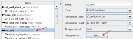
Description Due to a problem in the Quartus ® Prime Pro Edition starting since software version 24.1, the Agilex ® 5 and Agilex ® 3 FPGA EMIF IP is missing from the BSP Linker when generating the Board Support Package. This might occur for Nios ® V processor designs targeting Agilex 5 FPGA or Agilex 3 FPGA, that uses EMIF IP. This is because Agilex 5 and Agilex 3 FPGA EMIF IP are missing the isMemoryDevice agent information. Refer to Nios® V Processor Software Developer Handbook - Memory-Mapped Slave Information (PDF) for information about isMemoryDevice agent information. Refer to External Memory Interfaces (EMIF) IP User Guide Agilex® 5 FPGAs and SoCs (PDF) for information Agilex ® 5 FPGA EMIF IP. Refer to External Memory Interfaces (EMIF) IP User Guide Agilex® 3 FPGAs and SoCs (PDF) for information Agilex ® 3 FPGA EMIF IP. Resolution To work around this problem in the Quartus ® Prime Pro Edition in all the affected software version, apply either one of the following workarounds: Workaround 1: Manually add isMemoryDevice to the EMIF IP (in Platform Designer only) Select the s*_axi4 signal (mainband AXI4 from fabric to controller) that connects to the Nios ® V processor’s instruction/data manager. Right-click, and click Edit Component Instantiation ... Select s*axi4 and edit the Assignments. Enter new Key as embeddedsw.configuration.isMemoryDevice, and Value as 1. Save the new assignment. Generate a new BSP. Workaround 2: Manually define EMIF IP linker memory device Refer to the Nios V Embedded Processor Design Handbook - Defining Address Span Extender Linker Memory Device. The example demonstrates how to manually define Address Span Extender linker memory device. For this problem, apply the same procedure but on the EMIF IP directly. This problem is currently scheduled to be resolved in a future release of the Quartus ® Prime Pro Edition Software. Related Articles LPDDR4 not available in NIOS® V/g linker script - Agilex® 5 FPGA, Quartus® 26.1 Pro Issue with BSP Creation for Nios® V/m Using LPDDR4 on Agilex® 5 FPGA (Quartus® 24.1 & 24.3.1)147Views0likes0CommentsWhich LPDDR5 WCK:CK ratio is supported in Agilex® 7 FPGA M-Series and Agilex® 5 FPGA devices?
Description External Memory Interfaces (EMIF) IP of Agilex® 7 FPGA M-Series and Agilex® 5 FPGA devices only supports WCK:CK ratio of 4:1. Resolution WCK:CK ratio of 2:1 is not supported.61Views0likes0CommentsWhy is the FPGA To HPS bridge not functional in a non-HPS EMIF hardware design in Agilex® 5 FPGA device in 25.3.1 release and earlier?
Description Due to an incorrect configuration in the mpfe_config register in the System Manager, performed by the SDM FW, the FPGA-to-HPS transactions will fail to complete on the Agilex® 5 FPGA device in a hardware design that does not instantiate the HPS EMIF IP created with Quartus® Prime 25.3.1 and before. The problem resides in the incorrect value that the SDM FW assigns to the mpfe_config[f2soc_intfcsel] bit when the HPS EMIF is not instantiated. Under this scenario, it is expected that the f2soc_intfcsel field has a value of ‘1', but this is set to '0’ instead. Resolution To workaround this problem, you can set the mpfe_config[f2soc_intfcsel] bit to '1' in the FSBL. The following snippet shows an example of how to do it in U-Boot SPL: #define MPFE_CONFIG_F2SOC_INTFCSEL_BIT 0 void board_init_f(ulong dummy) { : setbits_le32(socfpga_get_sysmgr_addr() + SYSMGR_SOC64_MPFE_CONFIG, BIT(MPFE_CONFIG_F2SOC_INTFCSEL_BIT)); do_bridge_reset(1, RSTMGR_BRGMODRST_FPGA2SOC_MASK ); : } This needs to be done before the FPGA-to-HPS (F2H) bridge is released from reset. This problem will be fixed in a future release. Note: If your non-HPS EMIF design instantiates the Altera ACE5-Lite Cache Coherency Translator (CCT) and, after applying the above workaround, you observe that read transactions in the FPGA-to-HPS (F2H) bridge succeed, but after a write transaction, the system hangs, you may require an additional fix in the ACCT IP that will be released together with the mpfe_config[f2soc_intfcsel] configuration fix. Please refer to Why does the Agilex® 5 FPGA Hard Processor System hang during ACCT IP operations when translating AXI4 to ACE5‑LITE?80Views0likes0Comments