configuration
1094 Topics
Three 9x9 multipliers in one DSP
Hello everyone, Do have somebody the project example with three 9x9 multipliers in one DSP looks like in this post: How to configure DSP block in "three 9x9 multipliers" mode? | Altera Community - 90399 I tired to do this project and I have got one mult. per DSP.11Views0likes1Comment
DK-DEV-AGI027RBES CXL Type-3 example remains in reset and is not detected by host
Hi, I have several Agilex 7 FPGA I-Series Development Kits with serial numbers 8100035 and 8020138. My goal is to run the boards as CXL Type-3 devices and verify that they can be enumerated by the host. I am currently debugging board 8020138 with the following setup: Board: DK-DEV-AGI027RBES FPGA: AGIB027R29A1E2VR3 Power configuration: Power Solution 2 Quartus Prime Pro: 24.3 Connection: PCIe edge connector Design: CXL Type 3 with DDR4 Link width: CXL x16 Number of slices: 2 PLD clock: 400 MHz Reference clock mode: Common Refclk source is global clock: Enabled The board can successfully enumerate as a normal PCIe endpoint when using the pcie_ed example design included in: agilex_agib027r29a1e1vb_fpga_revc_v24.3b194_v1.1 However, when I generate and compile the RBES CXL Type-3 DDR4 example design, the host cannot detect the device and it does not appear in lspci. I added JTAG debug registers and Signal Tap probes. The observed status is: config_done = 1 pll_lock = 1 sip_rst_n = 0 cxl_warm_rst_n = 0 cxl_cold_rst_n = 0 ip2hdm_reset_n = 0 ip2cafu_avmm_rstn = 0 ip2csr_avmm_rstn = 0 pf0_bus_master_en = 0 pf0_memory_access_en = 0 pf0_msix_enable = 0 The fabric heartbeat counter(refclk4) is running, so FPGA configuration and the debug fabric clock are working. However, the CXL cold, warm, and SIP resets never deassert, and host enumeration never starts. Could you please confirm: Are these CXL IP settings correct for board 8020138, Power Solution 2, and the PCIe edge connector? For CXL x16 with two slices, must both refclk0 and refclk1 be active? What conditions control cxl_cold_rst_n, cxl_warm_rst_n, and sip_warm_rstn_o? How can I observe the physical PERST# status, R-Tile reset status, PHY initialization status, LTSSM state, and link-up status? Should Enable PIPE Mode Simulation be disabled for hardware operation? Is 400 MHz the correct PLD clock frequency? Is there a known-good CXL Type-3 DDR4 example project or SOF for DK-DEV-AGI027RBES with FPGA AGIB027R29A1E2VR3? Are there any required Quartus 24.3 patches for this board and CXL IP? The normal PCIe example works, but the CXL example remains in reset. This suggests the issue may be related to the CXL IP configuration, reference-clock/reset requirements, or the generated example-design constraints. I can provide the IP configuration, QSF/SDC files, Signal Tap captures, compilation logs, and host logs if needed. Thank you. Best regards, Jeffrey27Views0likes1Comment
Build error on tutorial, missing CMakeLists.txt
I previously built the tutorial helloworld project with no errors. I then made small changes to the BSP generation settings and re-generated the BSP. I did not try to re-import the BSP code into my project because it was already imported. I immediately re-built the whole project in RiskFree, I get the following error: CMake Error: The source directory "C:/fpga_projects/an985/helloworld" does not appear to contain CMakeLists.txt. I verified that there is no CMakeLists.txt file in the folder C:/fpga_projects/an985/helloworld. This is because that folder contains a subfolder Software which has subfolders for hal_app and hal_bsp, each of which contains their own CMakeLists.txt file. Where would I change a file or a configuration so that the build knows there there are two subprojects, each with their own CMakeLists.txt file? See attached screenshot of folders and files.60Views0likes1Comment
FPGA simulation and real HW behavior discrepancy
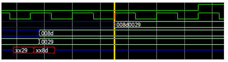
Dear Altera Quartus 18.1 sim lib could try 20.1 or newer but not sure this is due to Quartus version as it is sim lib. I am encounter an unexplainable experiment result that contradicts simulation and real HW. Background when interfacing a DQS DQ readout a IDDR with CCD sync flops are used. For these primitives, it should expected 1 + 2 and clock +ve edge should expect data push out. [A] This can simply considered as early push out but it should not act as such. With the use of "__ALTERA_STD__METASTABLE_SIM" we expected some metastable on the output. [B] Now things are more reasonable where 2 +ve clocks are expected. If we consider a full data w/o xx, things become unrecognizable. [C] The most interesting part when apply on real HW, it do produce correct data and the latencies do obeyed. altddio_in#( .intended_device_family ( "Cyclone IV E" ), .invert_input_clocks ( "ON" ), .lpm_hint ( "UNUSED" ), .lpm_type ( "altddio_in" ), .power_up_high ( "OFF" ), .width ( 8 ) )ddi_d_l( .aclr (reset), .datain (foo[7:0]), .inclock (bar[0]), .dataout_h (foobar_h[0+:8]), .dataout_l (foobar_l[0+:8]), .aset (1'b0), .inclocken (1'b1), .sclr (1'b0), .sset (1'b0) ); + altera_std_synchronizer_bundle#( .width (foobar_bw *2), .depth (2) )async_flops( .clk (clock), .reset_n (~reset), .din (foobar), .dout (foobar_ccd) );100Views0likes1Comment
IS25LP064A interface with Cyclone V HPS
Hi all, has anyone tried accessing serial NOR flash IS25LP064A using QSPI driver within hwlib ? I have successfully performed initialisation, setup device configuration. The problem is that a read attempt (Normal Read and Fast Read) after executing erase sequence returns all zeros instead of all ones. has anyone else faced similar issue ? Best Regards Naresh82Views0likes4Comments
Introducing the Altera Community AI Responder — Beta
Altera is introducing the AI Responder, an assistant built into the Altera Community to help provide faster, context-aware guidance for Altera product questions. It uses relevant public Altera documentation and Knowledge Database content, with coverage continuing to expand. The AI Responder may provide source references and can hand off complex or out-of-scope questions to an Altera subject-matter expert. As a beta feature, responses may contain errors or omissions, so please review the sources and verify technical guidance against official Altera documentation before implementation. If the response does not fully address your question, add more context and tag ai_responder to continue the discussion. We welcome your feedback as we improve the Community experience.26Views0likes0Comments