Altera_Forum Honored Contributor
Honored ContributorHonored ContributorI wanted to know if anyone has used the Altera Stratix4GX PCIe card as
a root port. I have used it as endpoint but have not used as a root- port. As an endpoint all I have to do is plug in the card to a motherboard. But as a root-port, it needs to send out the requests to end point.Honored ContributorSo you have to build your own motherboard or use a eval card that has a PCIe socket to let another PCIe card connect to your root port.
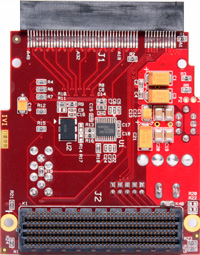
E.g., look at that board: altera stratix iv gx/gt pci express gen 2 / usb 3.0 / sfp+ development platform (http://www.hitechglobal.com/boards/stratix4gx.htm) from hitech global (http://www.hitechglobal.com). http://www.hitechglobal.com/images/S4GX-PCIE.jpg It has a general-purpose connector on top which allows for adapters to be used. One of these is a PCIe plug adapter called »FMC daughter card with x8 PCI Express Root«: http://www.hitechglobal.com/images/PCIExpress_FMC_f.jpgHonored ContributorThanks for getting back to me. In my application, I want to use the Altera Stratix4GX as the main rootport. I would like to feed the TLPs to it using Avalon Streaming interface which then is sent out to all other PCIe devices on the motherboard.
So in my application, the block diagram will look like as below: Processor --> Altera Stratix4gx root port --> Root port on the motherboard --> Reset of the devices on the motherboard. I notice that the Altera Stratic4gx root port has Base address register, That filters out only specific requests (?) In my application I need the ability to send out any cycles from processor to the root port on the motherboard via the Stratix4GX Root port. Is that possible? I am bit confused about having BAR in root port which limits this? Thanks for prompt response.Honored ContributorI would be surprised if you can put a root port on a PCIe expansion card handled by a root port on the motherboard, so the answer is: No, it’s not possible.
As written, the only way to make use of a root port in an FPGA is to drive another end point, or a switch with multiple end points behind it, when connected properly using such a dev kit with a PCIe socket card. Or you can build your own motherboard. edit: Maybe you meant something different? You don’t have to be a root port to send out requests on PCIe, but you have to have OS driver support to have proper I/O to I/O communication between your device and another end point. Most of the time it’s easier to let the devices communicate just with the main processor behind the motherboard root complex which then orchestrates data transfers using OS drivers. Only very high I/O rates or low-latency applications require direct device-to-device communication.Honored ContributorHonored ContributorHonored ContributorYou cannot connect your root port in the Stratix4GX with the root port on the motherboard. There must be only/exactly one root complex in the PCIe fabric, just like in PCI where you can also have just one root complex that drives DEVSEL#, etc. Please refer to PCIe Spec Section 1.3 »PCI Express Fabric Topology«.
Again, it’s not possible the way you want it. You can only drive your own, separate PCIe link as a root port as described above: Design a motherboard with your Stratix4GX as the root port, and it will work. But I’m still not convinced that a root port is what you really want to instantiate. As an endpoint in a PCIe slot, you can act as a bus master and issue DMA transfers on your own, issued by your CPU. But you cannot be another root port. Period. I cannot help you for the BAR question as I am not into root port design.Honored ContributorHonored ContributorYou can’t not use the main processor on the mainboard. You can’t re-route the the root port activity to a processor behind a PCIe link. All PCIe activity is initiated by the operating system on the CPU behind the root complex, and that’s only the main CPU on the base board.
If you really want/need to have a custom processor act as the PCIe root device, you have to build your own motherboard. Especially, if you want to use a standard COTS chipset you have to mimic the matching CPU local bus (or HyperTransport, etc.), but then you don’t need the PCIe root port in the FPGA in the first place. PCIe is strictly top–down. On top there is the root port, below are end points and switches. No way you can “reverse polarity” on a link and let an end point act as a super-root complex, disabling the main CPU.Honored ContributorIn that case, how does the PCIe speedbridge work? The PCIe speedbridge connects the processor to a chipset rootport. This device is completely transaparent to the OS and driver. It must be all custom and does not really leverage the hard IP?
Honored ContributorHaven’t heard of speedbridge yet. Interesting stuff. here are the docs (http://www.cadence.com/rl/resources/datasheets/sb_express_ds.pdf).
I think you misinterpret its function, though. The device can emulate two different things: (a) a PCIe end point, transparently visible to the PC the speedbridge is plugged into. (b) a PCIe root port when connected to a nice little board (the one with the blue-colored frame) with two sockets, probably connected 1:1, where the second plug is for a PCIe adapter card (e.g. SATA, USB3, 10G Ethernet) you want to test your root port against. The docs don’t speak – not even suggest – that the speedbridge can act as a root port, connected to a PC’s chipset root port. The specified transparency relates to the use of the drivers running on the PC running the speedbridge card in endpoint mode, emulating the real device function.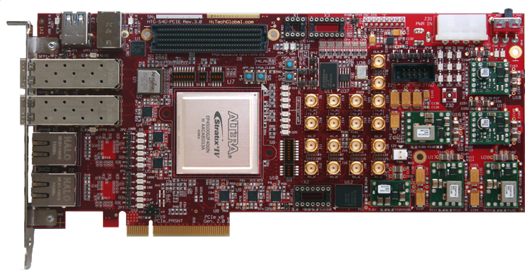