Forum Discussion

 New Contributor
Request about FPGA 10CL025YU256A7G

 Community Manager
This is a real hardware limitation, not an incomplete IBIS file. Let me explain what the Cyclone 10 LP handbook documents for the 3.3 V I/O standards and why you're seeing exactly three models.
Documented drive-strength options are genuinely limited at 3.3 V
The Cyclone 10 LP Core Fabric and General Purpose I/Os Handbook explicitly lists only the following current-strength settings for the 3.3 V standards:
- 3.3 V LVCMOS: IOH/IOL current strength = 2 mA only Cyclone 10 LP Core Fabric and General Purpose I/Os Handbook
- 3.3 V LVTTL: IOH/IOL current strength = 8 mA and 4 mA Cyclone 10 LP Core Fabric and General Purpose I/Os Handbook
Your IBIS file (cmos33_cio_d2, ttl33_cio_d4, ttl33_cio_d8) maps exactly to these three documented settings — so the IBIS file is complete and accurate; there are no hidden higher-drive-strength 3.3 V models to be found.
Compare this to lower-voltage standards, which have significantly more options:
- 1.8 V LVTTL/1.8 V LVCMOS: 16, 12, 10, 8, 6, 4, 2 mA Cyclone 10 LP Core Fabric and General Purpose I/Os Handbook
- 2.5 V LVTTL/2.5 V LVCMOS: 16, 12, 8, 4 mA Cyclone 10 LP Core Fabric and General Purpose I/Os Handbook
- 3.0 V LVTTL/3.0 V LVCMOS: 16, 12, 8, 4 mA Cyclone 10 LP Core Fabric and General Purpose I/Os Handbook
The underlying reason is the I/O transistor technology: the Cyclone 10 LP devices use TSMC 2.5 V transistor technology in the I/O buffers, though the devices are compatible with 2.5 V, 3.0 V, and 3.3 V configuration voltage standards. Cyclone 10 LP Core Fabric and General Purpose I/Os Handbook Operating the I/O buffers at 3.3 V is at the ceiling of what these transistors support, which constrains both the number of drive-strength taps and maximum achievable output current.
Slew-rate control is also not available at 3.3 V
The slew-rate control table in the handbook covers 3.0 V LVTTL/LVCMOS and below — there is no 3.3 V LVTTL entry in that table. This explains why your 3.3 V IBIS models carry no slow/medium/fast suffix variants: programmable slew rate control is a supported feature for optimizing signal integrity, Cyclone 10 LP Core Fabric and General Purpose I/Os Handbook but it is not available for the 3.3 V standards on this device.
For reference, slew rate control is confirmed for:
- 3.0 V LVTTL/3.0 V LVCMOS: slew rate control at 16, 12, 8 mA Cyclone 10 LP Core Fabric and General Purpose I/Os Handbook
- 2.5 V LVTTL/2.5 V LVCMOS: slew rate control at 16, 12, 8 mA Cyclone 10 LP Core Fabric and General Purpose I/Os Handbook
- 1.8 V LVTTL/1.8 V LVCMOS: slew rate control at 16, 12, 10, 8 mA Cyclone 10 LP Core Fabric and General Purpose I/Os Handbook
Practical implications for your 166 MHz DDR QSPI design
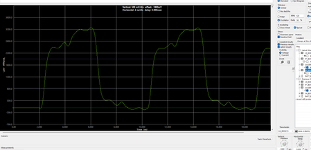
The slow rise/fall times you are observing (>1 ns even at 120 MHz with ttl33_cio_d8) are a direct consequence of this hardware constraint: 8 mA is the maximum available drive strength at 3.3 V, and there is no fast-slew-rate option. Achieving clean signal integrity at 166 MHz DDR with this driver is going to be very challenging on anything but a very short, lightly loaded trace.
My recommendation: if your QSPI flash device and board design can tolerate it, consider switching VCCIO to 2.5 V or 1.8 V. At 2.5 V you gain access to 16 mA drive with slew-rate control, and at 1.8 V you get up to 16 mA with slow/medium/fast slew-rate variants — exactly the richer model set you observed in the IBIS file. The current strength setting is what the output buffer is guaranteed to drive at the switching thresholds of the I/O standard — for example, a buffer with an 8 mA setting will drive at least 8 mA at the minimum VOH and maximum VOL for the standard. To verify the actual current for your specific board topology, running IBIS simulations is recommended. Does the current strength of an output buffer refer to the maximum current that the buffer is able to drive out?
If 3.3 V is a hard requirement, your best path is board-level optimization: minimize trace length and loading, use matched termination to control reflections and reduce the effective slew-rate requirement on the driver, and validate carefully with IBIS simulation as the ttl33_cio_d8 model is the highest-fidelity option available for that voltage.
Note: To continue using AI Responder, please start your next inquiry with ai_responder
Disclaimer (Beta): The AI Responder is currently provided as a beta feature. AI-generated responses may contain errors or omissions. Please verify technical guidance with official Altera documentation before implementation.
Thank you very much.


