Forum Discussion

 Occasional Contributor
Timing failure with external synchronous SRAM
- 2 years ago
Sorry for the delay in response. Been taking some time to solve the timing violation.
For bidirectional I/O, they are analyzed as inputs and outputs, so they usually have both set_input_delay and set_output_delay assignments.
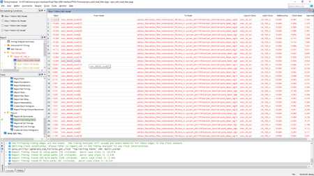
These sdc below in the project could be reason we got the huge negative slack. The tool analyze that the Data Arrival Path goes from clk_100_in -> sram_clk_out -> sram_clk_inout (o) -> external device -> sram_clk_inout (i) and then back to RAM block. This make it a very long timing path.
set_input_delay -clock sram_clk_out -min 1.3 [get_ports {sram_data36_inout*}]

set_input_delay -clock sram_clk_out -max 3 [get_ports {sram_data36_inout*}]
With that, I create a virtual clock and add the input and output delay constraint to the sram_data36_inout*:
create_clock -name {sram_clk_ext} -period 10.000ns

set_input_delay -clock sram_clk_ext -min 1.3 [get_ports {sram_data36_inout*}]
set_input_delay -clock sram_clk_ext -max 3 [get_ports {sram_data36_inout*}]

set_output_delay -clock sram_clk_out -min 1.3 [get_ports {sram_data36_inout*}]
set_output_delay -clock sram_clk_out -max 3 [get_ports {sram_data36_inout*}]
I also disable all the location assignment so that the fitter can place and route without being constraint, to meet the timing.
Attached the modified project. Though there is a timing violation of sram_address21_out and I believe it can be solved by tweaking the -max value to 1.0.
set_output_delay -clock sram_clk_out -max 1.0 [get_ports {sram_*_out*}]Best Regards,
Richard Tan

 Super Contributor
Hi,
Do you able to provide the information from my previous questions?
Thanks.
Best Regards,
Richard Tan
 arno_va2 years ago
Dear Richard,
Sorry for my delayed response. Here are the answers you've requested:
1) I'm not sure whether I understand your question correctly but I think the answer is yes. The data-bus to the ZBT SRAM is bidirectional so I need to constrain both outgoing and incoming data (and control signals).
2) The 100 MHz (XOSC) system clock of the FPGA is used for this. It's simply forwarded in the FPGA from "clk_100_in" to "sram_100_clkout".
3) This is a (simplified) block diagram of the (SRAM)-design I'm doing. It's pretty straightforward (imho):
4) For now I assume zero trace-delay etc. for the SRAM since the PCB design hasn't been done yet AND the SRAM will be near the FPGA so the trace delays etc. will be negligible compared to the requirements of the SRAM itself. So for now I take into account the SRAM's "Data output hold after CLK rise " which is 1.3 ns and "Data output valid after CLK rise" which is 3 ns. The sync. SRAM I'm using is a Cypress CY7C1470BV25
If you need to know anything else, let me know.
Thanks for your help.
Kind regards,
Arno


