Forum Discussion

 Occasional Contributor
Timing failure with external synchronous SRAM
- 2 years ago
Sorry for the delay in response. Been taking some time to solve the timing violation.
For bidirectional I/O, they are analyzed as inputs and outputs, so they usually have both set_input_delay and set_output_delay assignments.
These sdc below in the project could be reason we got the huge negative slack. The tool analyze that the Data Arrival Path goes from clk_100_in -> sram_clk_out -> sram_clk_inout (o) -> external device -> sram_clk_inout (i) and then back to RAM block. This make it a very long timing path.
set_input_delay -clock sram_clk_out -min 1.3 [get_ports {sram_data36_inout*}]

set_input_delay -clock sram_clk_out -max 3 [get_ports {sram_data36_inout*}]
With that, I create a virtual clock and add the input and output delay constraint to the sram_data36_inout*:
create_clock -name {sram_clk_ext} -period 10.000ns

set_input_delay -clock sram_clk_ext -min 1.3 [get_ports {sram_data36_inout*}]
set_input_delay -clock sram_clk_ext -max 3 [get_ports {sram_data36_inout*}]

set_output_delay -clock sram_clk_out -min 1.3 [get_ports {sram_data36_inout*}]
set_output_delay -clock sram_clk_out -max 3 [get_ports {sram_data36_inout*}]
I also disable all the location assignment so that the fitter can place and route without being constraint, to meet the timing.
Attached the modified project. Though there is a timing violation of sram_address21_out and I believe it can be solved by tweaking the -max value to 1.0.
set_output_delay -clock sram_clk_out -max 1.0 [get_ports {sram_*_out*}]Best Regards,
Richard Tan


 Super Contributor
The massive clock skew is definitely the problem and it's because you've defined your launch clock at the output of the FPGA, which is correct, but you've included the clock path delay through the device in the calculation. This is basically a data feedback design.
Your base clock and generated clock constraints are correct, but you need to false path to the clock output port:
set_false_path -to [get_ports sram_clk_out]
This is the same thing you do whenever you have an output clock, like if it's used for an SDR or DDR interface.
All the required data arrival components are part of the numbers you use for calculating set_input_delay max and min (clock path delay from the FPGA, the SRAM output's tco, and the data trace delay), so just removing the data analysis from the internal clock path with set_false_path (removes data path analysis but maintains clock path analysis) should do the trick.
 Occasional Contributor
Thanks for your reply. I've tried your suggestion (adding the false-path for sram_clk_out) and it doesn't seem to make any difference unfortunately. A few other things I've tried:
- I tried NOT forwarding the SRAM-clock through the FPGA (and connecting it directly from the XO to the SRAM clock input externally but that didn't fix my issue either);
- Using DCFIFO's instead of SCFIFO to allow one side to operate at clk_100_in and the other side on sram_clk_out but that didn't fix it either.
- Adding an extra input register for sram_data36_inout, again without any luck.
Do you have any other suggestions? Please note that (obviously) "clk_100_in" is also used for all the other logic in the FPGA, not just the SRAM-interface.
- sstrell2 years ago
When you say adding the false path didn't make any difference, can you explain? Did you recompile the design and rerun the timing analysis? Show your updated .sdc and a detailed slack path report (including the data path and the waveform view) for a path that is still failing.
- arno_va2 years ago
Yes I recompiled the design and reran the timing analysis.
My (relevant sections of) sdc now looks like:
create_clock -name "clk_100_in" -period 10.000ns -waveform { 0.000 5.000 } [get_ports {clk_100_in}]
create_generated_clock -name {sram_clk_out} -source [get_ports {clk_100_in}] [get_ports {sram_clk_out}]
# SRAM input minimum delay in ns
set_input_delay -clock sram_clk_out -min 1.3 [get_ports {sram_data36_inout*}]

# SRAM input maximum delay in ns
set_input_delay -clock sram_clk_out -max 3 [get_ports {sram_data36_inout*}]

# SRAM output minimum delay (=hold time) in ns
set_output_delay -clock sram_clk_out -min -0.5 [get_ports {sram_address21_out*}]
set_output_delay -clock sram_clk_out -min -0.5 [get_ports {sram_data36_inout*}]

# SRAM output maximum delay (=setup time) in ns
set_output_delay -clock sram_clk_out -max 1.5 [get_ports {sram_address21_out*}]
set_output_delay -clock sram_clk_out -max 1.5 [get_ports {sram_data36_inout*}]

set_false_path -to [get_ports sram_clk_out]
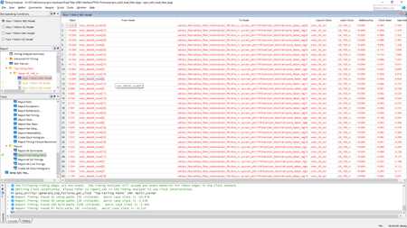
And my failing paths now look like:
and d31's timing report looks like:
Let me know in case you need additional info. I have a feeling Quartus is having a hard time getting the timing right for sram_data36_inout input-path vs. output-path. What do you think?


