Forum Discussion

Gonza New Contributor
28 days agoNew ContributorAgilex 5 FPGA EMIF: sharing LPDDR4 reference clock between Bank 3A and Bank 3B
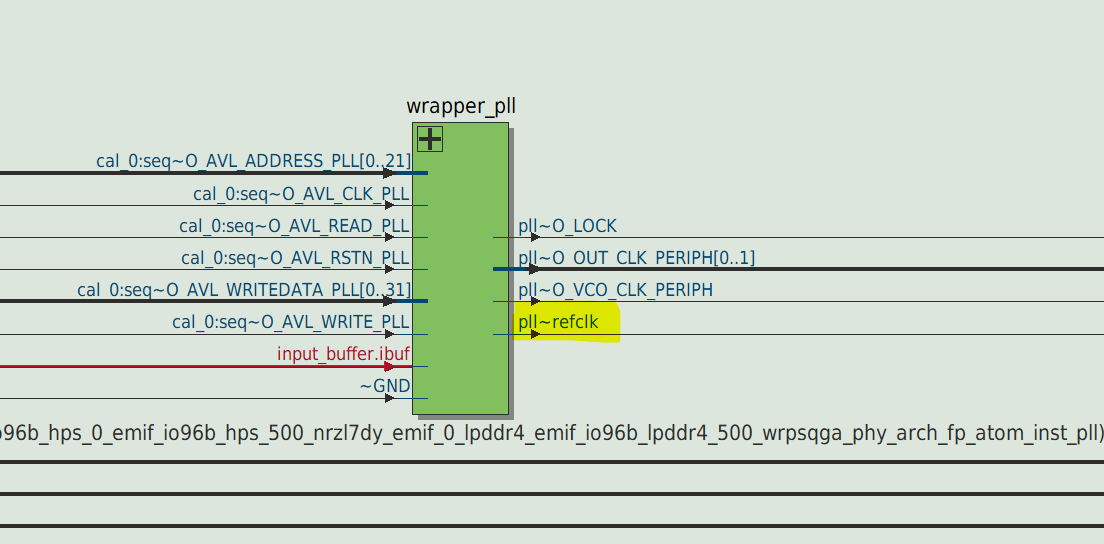
Hello, I'm working with an Agilex 5 E-Series A5ED043BB32AI4S device. On my board, I have two 32-bit LPDDR4 interfaces connected to the HSIO banks 3A and 3B. The DDR reference clock is available only...
 24 days ago
Hi Gonza ,
- For the FPGA LPDDR4 External Memory Interfaces (EMIF) IP, is it mandatory that the PLL reference clock be located in the same bank as the EMIF instance?
- We recommended to have the refclk placed within the Address and Command Group of each interface.
- While sharing PLL reference clock within an IO Bank is still permitted.
- Is there any supported mechanism to share or bypass the PLL reference clock from the EMIF PLL in bank 3A to the EMIF PLL in bank 3B, similar to what appears to be done automatically by the HPS EMIF 2x32 implementation?
- You can use clock bridge IP to supply the clock to both EMIF interfaces across the banks.
- If you still facing the issue, please share the example design for debugging purpose.
Regards,
Adzim
- For the FPGA LPDDR4 External Memory Interfaces (EMIF) IP, is it mandatory that the PLL reference clock be located in the same bank as the EMIF instance?

sstrell Super Contributor
27 days agoSuper Contributor- To do this, the EMIF I/O sub-banks must be "adjacent" to each other. Yes I/O banks 3A and 3B are physically adjacent to each other, but the I/O sub-banks must be adjacent for this to work and that means the "top" sub-bank (closest to the device edge) in 3A is adjacent to the "bottom" sub-bank (away from the device edge) in 3B, so you have to use these two particular sub-banks. Easiest way to make sure you set this up correctly is to use Interface Planner.
- I think the HPS PLL reference clock setup is unique. For standalone EMIF, you have to place in the appropriate sub-banks as I just mentioned to share the clock or drive the clock in to each interface separately from elsewhere.