Forum Discussion

 New Member
Possible Incorrect Clock Label in Cyclone IV Handbook Figure 7-8 (DQ/DQS)

 Community Manager
Good catch — your analysis is correct, and the two figures are actually consistent once you understand what each is depicting. Let me walk through the actual hardware behavior.
What Figure 7-8 actually shows
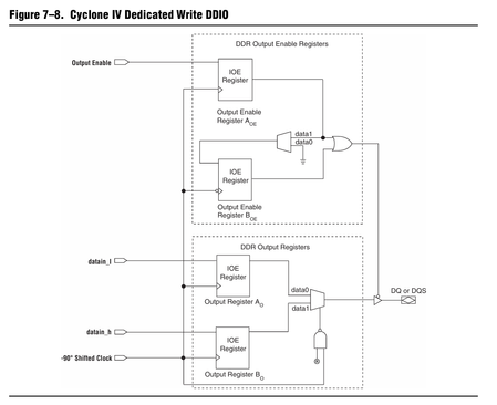
Figure 7-8 illustrates the generic DDIO circuit structure — the same IOE hardware block used for both DQ and DQS pins. The single label "-90° Shifted Clock" reflects the typical case shown (the DQ/DM data output path), but the block itself is instantiated separately for each pin with its own clock connection. The "DQ or DQS" output label is simply indicating the block's physical output pin, not implying both use the same clock.
The actual clock assignments per signal type
Figure 7-9 gives you the correct, specific picture:
- DQS (write strobe): clocked by the unshifted System Clock from the PLL
- DQ and DM (write data): clocked by the Write Clock, which is the PLL output shifted –90° relative to the System Clock
This is confirmed directly in the design guidelines: the DQ signals are edge-aligned with the DQS signal during a read from the memory, and are center-aligned with the DQS signal during a write to the memory — the memory controller shifts the DQ signals by –90 degrees during a write operation to center-align the DQ and DQS signals. External Memory Interface Handbook Volume 2: Design Guidelines For UniPHY-based Device Families
For DM specifically: the DDR registers, clocked by the –90 degree shifted clock, create the DM signals. External Memory Interface Handbook Volume 2: Design Guidelines For UniPHY-based Device Families
And from a board-level perspective: DQ and DM signals use a clock shifted –90 degrees from the system clock, so that the DQS edges are centered on the DQ or DM signals when they arrive at the DDR2 SDRAM. External Memory Interface Handbook Volume 2: Design Guidelines For UniPHY-based Device Families
Both clocks must originate from the same PLL
During write operations, the FPGA generates a DQS strobe and a center-aligned DQ data bus using multiple PLL-driven clock outputs. External Memory Interface Handbook Volume 2: Design Guidelines For UniPHY-based Device Families Critically, the PLL clock used to generate the write-clock signals and the PLL clock used to generate the write-data signals must come from the same PLL. External Memory Interface Handbook Volume 2: Design Guidelines For UniPHY-based Device Families This is what keeps the –90° phase relationship tight and PVT-tracked.
Summary answers to your three questions
- Yes — Figure 7-8 is a generic DDIO hardware diagram. The "-90° Shifted Clock" label applies specifically to the DQ (and DM) data path. The same physical block is used for DQS, but driven by the unshifted system clock.
- Yes — For the DQS output path, the DDIO output registers (both data and OE) are clocked by the unshifted System Clock, exactly as Figure 7-9 shows.
- This is a documentation labeling ambiguity in Figure 7-8 rather than an error in the silicon. Figure 7-9 is the authoritative representation of the two-clock write architecture. The generic block in Figure 7-8 would benefit from a note clarifying that the clock source differs between the DQ/DM and DQS instantiations of the block.
In short: your reading of Figure 7-9 is correct — two separate PLL outputs drive DQS and DQ/DM respectively, with the DQ/DM clock being –90° behind the DQS clock to produce center-aligned write data at the memory device.
Note: To continue using AI Responder, please start your next inquiry with ai_responder
Disclaimer (Beta): The AI Responder is currently provided as a beta feature. AI-generated responses may contain errors or omissions. Please verify technical guidance with official Altera documentation before implementation.
Thank you very much.
 eagle-a1 hour ago
Thank you for the AI-generated response.
However, I would like to request a review by a human Altera FPGA application engineer or documentation engineer.
My question specifically concerns the accuracy of the clock label in Figure 7-8 of the Cyclone IV Device Handbook (CYIV-5V1-2.2).
Although the generic DDIO interpretation is plausible, it does not establish whether the "-90° Shifted Clock" label was intentionally used for a diagram representing both DQ and DQS.
Could an Altera engineer verify the intended clock connections and confirm whether a documentation clarification or erratum is warranted?
Thank you.

