Forum Discussion

 Contributor
Cyclone IV drop in replacement confirmations
 Contributor
The question is not related to any specific Cyclone IV devices:
The question is about when VCCIO is driven from 1.8V or any voltage under the VCCA, do the input pins are allow to feed in 2.5V or 3.3V as datasheet marked with <3.6V on inputs?
When this question is answered there is no issue on the remains drop-in compatibilities.
Thanks,
Brian

 Regular Contributor
Hi Brian,
These two devices should not be treated as drop-in replacements in this board condition. Cyclone IV supports vertical migration within the same package, but the migration devices must have compatible dedicated input pins, configuration pins, and power pins.
You can select migration devices in Quartus and check the Pin Migration view for pins whose functions change. The Fitter uses the selected migration-device list to restrict the design to compatible pins; pins that are power pins on one device should not be treated as usable user I/O across the migration path.
Reference: Device Migration Planning, AN 592: Cyclone IV Design Guidelines.
Maybe just for your information, I saw an old documentation, Quartus® II Handbook mentioning below statement:
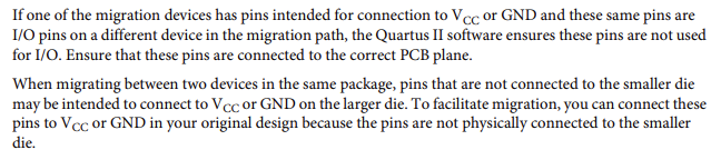
Regards,
Aqid
- BrianSune_Froum1 month ago
The table I attached is from the "Pin Migration view".
Yes datasheet Larger die -> smaller die migrate.
Which is understandable from the idea of 1.8V / 1.5V VCCIO minimum requirements so 1.2Vcore/GND is always treaded as input / HI-Z and does not contradicts the voltage requirements.
But the issue we are discussing is VCCA in that table which larger die have more PLL power pins.
So drop-in migration have no clear details on such.
3.6V is maximum input but VCCIO aka 1.8V vs 2.5Vcca fixed power pin require Altera to response the proper drop-in design/treatment.
Thanks,Brian
- AqidAyman_Altera2 hours ago
Hi Brian,
I really apologies for the delay answer. Our suggestion on how to treat this migration are:
1- Hard-tie it to 2.5 V on the board, and do not use it as functional I/O on the other density (reserve as input / unused).
2- On the voltage point: recommended VI goes up to 3.6 V, so 2.5 V is inside that absolute DC range.
Preferred options if the bank must stay 1.8 V: drop that density from the migration set, raise that bank’s VCCIO to 2.5 V if the whole bank allows it, or replan so the remapped power ball is not in an active 1.8 V bank.
Regards,
Aqid- BrianSune_Froum1 hour ago
AqidAyman_Altera
TBH: real HW testing is not going to tell it will break but long term consideration on those pin are more likely what we trying to concern and prevent.1- Hard-tie it to 2.5 V on the board, and do not use it as functional I/O on the other density (reserve as input / unused).
Q: Need more clarification on this: tri-state w/o pull-up or ?
Preferred options if the bank must stay 1.8 V: drop that density from the migration set, raise that bank’s VCCIO to 2.5 V if the whole bank allows it, or replan so the remapped power ball is not in an active 1.8 V bank.
I think this is impossible on SSTL or HSTL 1v8 where the output still requires to run from VCCIO supply.So after long period of time someone who's claim the datasheet with wrong table referring is a b.s. and yet the migration table from Quartus is not 100% best option from first place only a suboptimal way to mix from low to high density.


