Forum Discussion

 New Contributor
Agilex 5E: How to access FPGA-side EMIF DDR4 from HPS through HPS2FPGA?
 3 months ago
Hi amsssss123
Yes the hps2fpga_clk and the hps2fpga_rst are referencing to the hps2fpga_axi_clock and hps2fpga_axi_reset mentioned.
For the EMIF Clock in the first screenshot it is shows the Access Mode of the EMIF is in Sync Mode with a clock out present, it should be connected to the hps2fpg_clk.
If it is in Async Access Mode both hps2fpg_clk and s0_axi4_clk should be connected to the same clock source.
 New Contributor
Hi,
Thank you for the clarification!
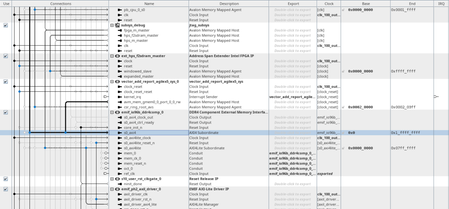
I updated the design according to your suggestion:
- emif_io96b_ddr4comp_0.s0_axi4_clock_out -> subsys_hps.hps2fpga_clk
- subsys_hps.h2f_reset -> subsys_hps.hps2fpga_rst
Could you please check whether my current connections are correct, and whether there are any other incorrect parts?
I have one follow-up question about the other HPS bridge clocks. For example, lwhps2fpga_clk is still connected to clk_100 in my design. This clock is used for lightweight HPS-to-FPGA accesses, such as CSR/control registers, not for the main EMIF s0_axi4 data path.
Is it okay for lwhps2fpga_clk and other unrelated HPS-side control clocks to remain on clk_100, even though hps2fpga_clk is now driven by emif_io96b_ddr4comp_0.s0_axi4_clock_out and therefore has a different frequency?
Thank you again for your help!
 Regular Contributor
Hi amsssss123
From the screenshot, the connections looks okay.
For the lwhps2fpga_clk, it could be connected to the clk_100 when the hps2fpga_clk is connected to a different clock.
- amsssss1232 months ago
Thank you very much for your help!

