Forum Discussion

 New Member
Agilex 5 FPGA EMIF: sharing LPDDR4 reference clock between Bank 3A and Bank 3B
Hello,
I'm working with an Agilex 5 E-Series A5ED043BB32AI4S device. On my board, I have two 32-bit LPDDR4 interfaces connected to the HSIO banks 3A and 3B. The DDR reference clock is available only on the dedicated differential CLK pins in bank 3A (K105/M105). There is no refclk in bank 3B.
HPS EMIF case
Using the External Memory Interfaces for HPS IP configured as 2x32 LPDDR4, Quartus instantiates two EMIFs (one in bank 3A and one in bank 3B).
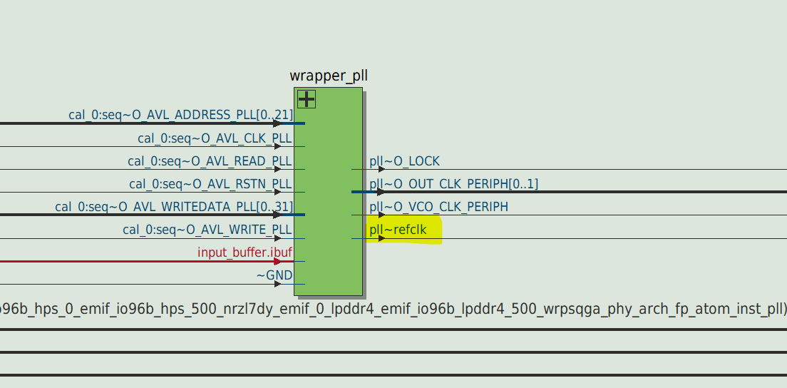
From the generated netlist (see attached images), it appears that the PLL associated with the EMIF in bank 3A receives the external CLK (K105/M105), the PLL reference clock is then internally forwarded/shared to the PLL associated with the EMIF in bank 3B. The design routes and fits successfully.
This is the intended DDR architecture on my board and works correctly.
FPGA EMIF case
For debug purposes, I would like to use the LPDDR4 External Memory Interfaces (EMIF) IP together with the EMIF Debug Toolkit. Since this IP only supports up to 1x32 LPDDR4, I instantiated one LPDDR4 EMIF in bank 3A and one LPDDR4 EMIF in bank 3B.
The EMIF in bank 3A works correctly when using the REFCLK in bank 3A (on K105/M105).
However, I cannot get the EMIF in bank 3B to fit when its PLL reference clock is assigned to the same REFCLK source located in bank 3A. The fitter reports routing/connectivity issues.
Questions
1) For the FPGA LPDDR4 External Memory Interfaces (EMIF) IP, is it mandatory that the PLL reference clock be located in the same bank as the EMIF instance?
2) Is there any supported mechanism to share or bypass the PLL reference clock from the EMIF PLL in bank 3A to the EMIF PLL in bank 3B, similar to what appears to be done automatically by the HPS EMIF 2x32 implementation?
Any guidance would be appreciated.
Thanks,
1 Reply
 sstrell
Super Contributor
- To do this, the EMIF I/O sub-banks must be "adjacent" to each other. Yes I/O banks 3A and 3B are physically adjacent to each other, but the I/O sub-banks must be adjacent for this to work and that means the "top" sub-bank (closest to the device edge) in 3A is adjacent to the "bottom" sub-bank (away from the device edge) in 3B, so you have to use these two particular sub-banks. Easiest way to make sure you set this up correctly is to use Interface Planner.
- I think the HPS PLL reference clock setup is unique. For standalone EMIF, you have to place in the appropriate sub-banks as I just mentioned to share the clock or drive the clock in to each interface separately from elsewhere.