Forum Discussion

Gonza New Member
1 day agoNew MemberAgilex 5 FPGA EMIF: sharing LPDDR4 reference clock between Bank 3A and Bank 3B
Hello, I'm working with an Agilex 5 E-Series A5ED043BB32AI4S device. On my board, I have two 32-bit LPDDR4 interfaces connected to the HSIO banks 3A and 3B. The DDR reference clock is available only...

sstrell Super Contributor
2 hours agoSuper Contributor- To do this, the EMIF I/O sub-banks must be "adjacent" to each other. Yes I/O banks 3A and 3B are physically adjacent to each other, but the I/O sub-banks must be adjacent for this to work and that means the "top" sub-bank (closest to the device edge) in 3A is adjacent to the "bottom" sub-bank (away from the device edge) in 3B, so you have to use these two particular sub-banks. Easiest way to make sure you set this up correctly is to use Interface Planner.
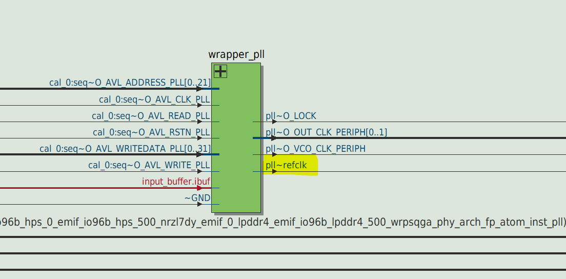
- I think the HPS PLL reference clock setup is unique. For standalone EMIF, you have to place in the appropriate sub-banks as I just mentioned to share the clock or drive the clock in to each interface separately from elsewhere.