Forum Discussion

Syuan_5728's avatar
Syuan_5728
Icon for New Contributor rankNew Contributor
2 years ago

DE10-nano FPGA write to HPS SDRAM controller

I am currently attempting to create an Avalon Master in the FPGA section on the DE10-nano board, and I'm trying to use the FPGA2HPS_sdram bridge to write data to the SDRAM controller in the HPS.

When I press the KEY button on the DE10-nano board, a write command will be sent to the SDRAM controller. The entire Avalon Master structure is very simple, as shown in the diagram below:

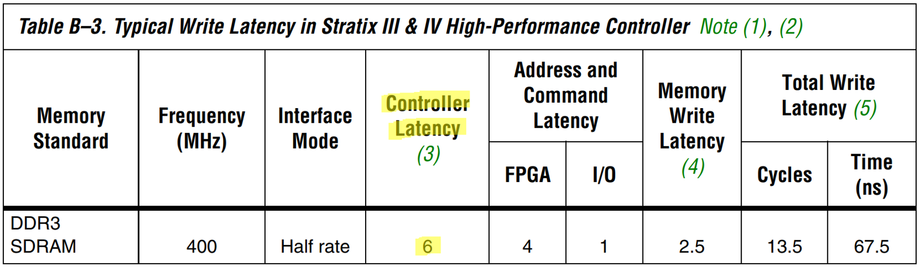
The strange thing is that when I send a write command, the SDRAM controller immediately raises the waitrequest signal to a high level. According to the Avalon protocol, the Master must keep the data unchanged, so the Master will endlessly wait since the waitrequest signal from the SDRAM controller will never return to a low level. When I ignore the waitrequest signal and change the write address and data according to the Master's clock cycle, I found that the SDRAM controller is actually writing data normally. The write cycle is 6 Master clock cycles. This has left me very puzzled. Has anyone encountered the same situation? Any insights would be greatly appreciated!

6 Replies

  • Hi,


    Before we continue investigate, may i know which baremetal application version (hwlib) are you using?

    and which link are you refer for your design example?


    Thank you,


    • Syuan_5728's avatar
      Syuan_5728
      Icon for New Contributor rankNew Contributor

      I have identified the reason. In fact, I found that using the SignalTap program the device, as well as converting the SOF to RBF and automatically programming it during Linux boot, result in different SDRAM controller response signals.

      My speculation is that when using SignalTap to program the device, the DDR3 SDRAM might be in standby mode or not operational. This means that the SDRAM controller cannot complete the requested write task, leading to the waitrequest signal being constantly high. On the other hand, the Linux system automatically initializes the DDR3 SDRAM, ensuring that everything I'm requesting operates smoothly. The only limitation is that I'm unable to observe the signal performance through SignalTap.

      However, of course, everything is just my speculation. I don't have enough evidence to prove this matter.

      I am a beginner in FPGA, so I have very little knowledge about what you mentioned regarding "hwlib". I don't know how to properly query the version I am using. All of my builds come from this GitHub repository:

      https://github.com/zangman/de10-nano/tree/master

      In short, what I want to do is read RF signals through an ADC, digitize the data, and write it into half of the SDRAM space as a buffer because the ADC operates at a high speed. At the same time, I want to run an embedded Linux system on the HPS. Within this Linux system, I aim to use BusyBox to query the ADC digitized data that has been written into the SDRAM.

      In fact, I have achieved this already, and I have also speculated about why there is a write occurring every 6 Avalon Master clock cycles. Now, I just want to clarify the details behind it.

      Thank you, and I apologize if my explanation was not thorough enough. I'm more than willing to provide additional clarification if needed. If you have any insights about this ADC write task or the technical details behind the 6 Avalon Master clock cycles to SDRAM controller, I would greatly appreciate it if you could explain further. Your assistance is sincerely appreciated!

  • Hi,


    Thanks for your clarification. How ever i don't instance answer, i will gather your info and get back to you


  • Hi


    Actually what happens is that the signal cannot access the memory because it has been used by linux


    That's why the signal tap won't work


    • Syuan_5728's avatar
      Syuan_5728
      Icon for New Contributor rankNew Contributor

      In fact, I have also had doubts about this reason. However, even after removing the SD card with the Linux boot program and restarting the power, SignalTap still shows the same response (the Waitrequest signal remains high).

      Moreover, I have followed the instructions in the provided GitHub link (https://github.com/zangman/de10-nano/blob/master/docs/FPGA-SDRAM-Communication_-Avalon-MM-Host-Master-Component-Part-3.md) to reserve 512MB of DDR3 SDRAM to prevent it from being occupied by Linux. So, this is still perplexing me.

      And indeed, while running the Linux system, I can use BusyBox to query that the data I need has been written into the reserved 512MB space.

      In any case, thank you for your assistance. I will continue to search for a reasonable answer.

  • p/s: If any answer from the Intel Support is helpful, please feel free to provide rating with 4/5 survey on the support provided.