nios cpu
179 Topics
NIOS V Core Not Recognized in RiscFree IDE 25.2.1 Run Configuration
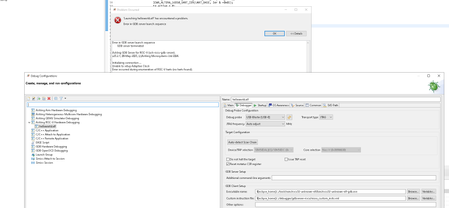
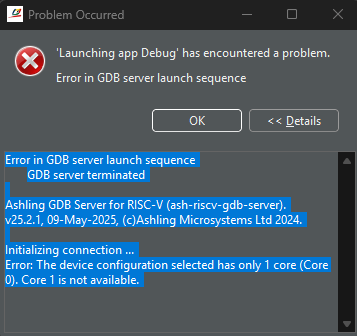
I am trying to run software that I developed using Quartus Prime Lite version 25.1 and RiscFree IDE version 25.2.1. However, in Run As > Run Configurations > Ashling RISC-V Hardware Debugging, the NIOS V core is not recognized in the Core Selection field under Target Configuration. The PIC is recognized correctly in the Device/TAP Selection field. I have found that this issue has occurred with some previous versions, but I would like to know whether this problem can also occur with RiscFree IDE version 25.2.1. If there is a known solution or workaround, I would appreciate any advice. I have attached screenshots of the issue for reference.34Views0likes2CommentsNios V XIP boot from UFM does not work with dual configuration on FPGA 10M50 Evaluation Kit
Hello, I am currently testing a project using Nios V on the "FPGA 10M50 Evaluation Kit". I am trying to boot the Nios V application from UFM using XIP (Execute In Place) with the dual configuration setting. However, I have not been able to successfully boot from UFM, even after checking the following items: * FPGA and board wiring * BSP Editor configuration * Standalone execution of the Nios V application (a simple LED blinking application) The Nios V application runs correctly as a standalone project, but it does not boot from UFM. I suspect that the issue may be related to my BSP Editor configuration. (I previously had some difficulties with a similar boot configuration when using Nios II.) I have attached my project files. If possible, could someone please review my project files and advise what might be causing the issue? *Note: The project was created under the D: drive on my PC.* ----------------------------------------------------------------------------------------------------------------- This is not directly related to the boot issue, but I also noticed another behavior with the Nios V application. When I tried to use "usleep()" in the application, the build completed successfully, but during execution the delay seemed to be ignored. If there is any required configuration or setting for "usleep()" to work correctly with Nios V, I would appreciate any advice. Thank you very much for your help.68Views0likes2Comments
Introducing the Altera Community AI Responder — Beta
Altera is introducing the AI Responder, an assistant built into the Altera Community to help provide faster, context-aware guidance for Altera product questions. It uses relevant public Altera documentation and Knowledge Database content, with coverage continuing to expand. The AI Responder may provide source references and can hand off complex or out-of-scope questions to an Altera subject-matter expert. As a beta feature, responses may contain errors or omissions, so please review the sources and verify technical guidance against official Altera documentation before implementation. If the response does not fully address your question, add more context and tag ai_responder to continue the discussion. We welcome your feedback as we improve the Community experience.18Views0likes0Comments
NIOS-V-64bit - why no double precision FPU ?
We need the 64 bit NIOS for several projects and must have a double precision FPU option. But the documentation so far lists only a single precision FPU Is this correct ? a 64 bit processor not having a (64 bit) double precision native FPU option seems unbeleiveable . It is about as strange as say, not having an 64 bit ALU. Altera- please explain ? page 3 : https://docs.altera.com/v/u/docs/759484/nios-v-processors-for-agilextm-5-fpgas-e-series-technology-brief Or please add this to the basic feature provision ? With thanks Glen. (Experienced Xilinx user consideriing migrating-defecting to Altera )Solved293Views0likes7Comments
Dual Port Nios V BSP error
I've created a Nios V qsys with dual port onchip memory in Quartus Pro 26.1 True dual port, first port connected to instruction manager, second - to data manager. Base addresses automatically assigned the same to both. But i'am unable to create the BSP due to memory regions overlapping error! Of course the addresses are same - its the same physical onchip memory! Any solytion, please? Regards, Vlad.229Views0likes5Comments
Nios V/g load-writeback hazard
Summary On a NiosV/g core, a long-latency load from an on-chip memory immediately followed by a short-latency load from the core's own TCM returns the TCM load's data in both destination registers. The first load's writeback is lost. lw a0, 0(t0) # t0 -> On-chip memory lw a1, 0(t1) # t1 -> DTCM (core-local) # a0 and a1 both end up holding the DTCM value Inserting a single instruction between the two loads is enough to avoid it. Two on-chip memory loads back to back are fine, and so is the reverse order (TCM load first, then the on-chip memory load). Minimal reproducer Assembly: _start: lui t0, 0x40 # t0 = 0x00040000 on-chip memory ("input memory") lui t1, 0x10 # t1 = 0x00010000 DTCM (core-local) lui t2, 0xe0 # t2 = 0x000e0000 2nd on-chip memory ("output memory") li a2, 0x47414c47 # a value distinct from the DTCM sentinel sw a2, 0(t0) # ...store it into input_mem nop # let the store retire. The hazard is about two nop # adjacent *loads*; keep everything else well nop # clear of the pair below so the test stays nop # unambiguous. lw a0, 0(t0) # long-latency load: on-chip memory (input memory) lw a1, 0(t1) # short-latency load: DTCM, immediately after sw a0, 0(t2) # output_memory[0] = result of the AXI load sw a1, 4(t2) # output_memory[1] = result of the DTCM load spin: j spin System details NiosV/g data_manager (AXI master) is directly connected to on-chip memories and pipeline stages are limited to 3 in Platform Designer.248Views0likes6Comments
Run-time errors using EMIF in Agilex 5 NIOS-V design
Hello, I am using Quartus Prime Pro 26.1.1, with the Agilex 5 development board (AXE5-Eagle). I am trying to run the NIOS-V code from the LPDDR4 memory, using JTAG to download/debug. The reset and exception vectors are set to the On-Chip RAM. I used the sample design provided for that board - AXE5 Eagle mipi_hdmi_mira220 and removed everything related to MIPI and HDMI. Added JTAG Uart IP. The resulting sample design is attached (mipi_hdmi_mira220.zip). In the software/ directory you can also see the FreeRTOS BSP I used. I created a simple FreeRTOS application that just prints some string to stdout. What I am seeing is - the RISC-V processor throws exceptions - one of the following - Misaligned Read Address, Misaligned Write Address or Invalid Instruction. This happens in alt_load_section(). If I execute step-by-step, no exception is thrown. But if I just run the application it fails. Is there something else that need to be added/updated/changed, in order to be able and execute code from LPDDR4 using the EMIF IP? I could not find any existing sample design, using NIOS-V and EMIF, with code execution from EMIF. Thank you, D.492Views0likes5Comments
Ashling RISC Free IDE fails to download ELF file
Hello ALTERA NIOSV Experts, I have been trying to execute an application using a NIOSV CPU with the Ashling RISC Free IDE. The problem is that when trying to download the elf file to a MAX10 ALTERA Development board i see an error message saying that the AShling IDE cannot determine the JTAG clock speed. I have added a Screen shot showing this event. Can anyone please suggest a solution to try ? I am currently using an ALTERA USB Blaster to connect but i have just ordered a USB Blaster II as i believe that can connect at faster clock speeds and is also more reliable. Thanks for any help,757Views0likes14CommentsNios IDE CPU Detection
Hi, I am trying to create bsp and software for Nios V , using Eclipse IDE. When specifying a new projcet and its .sopc file i see message CPU not detected. And i also see message the NIOS_EDS environment variable not set. See screen shot attached . I verified via command prompt the environment variable is set and can be verified. Also i noticed there are no examples installed at this path : C:\intelFPGA_lite\24.1std\nios2eds Looking forward to resolve these issues, Thanks, Regards,173Views0likes4Comments
not able to use multiple niosV cores at the same time
when I run ultiple niosV cores at the same time im not able to acess each of them even though i am able to detect them , i am faced with even though detecting gives me and i am unable to use the cores likewise this is my file on platform designer274Views1like7Comments